Self-driven MSM ultraviolet detector and preparation method thereof

An ultraviolet detector, self-driven technology, applied in the direction of semiconductor devices, final product manufacturing, sustainable manufacturing/processing, etc., can solve the problems of low responsivity, low current, low collection efficiency, etc., and achieve the effect of separation promotion

Pending Publication Date: 2022-05-24
NINGBO INST OF MATERIALS TECH & ENG CHINESE ACADEMY OF SCI
View PDF0 Cites 2 Cited by
  • Summary
  • Abstract
  • Description
  • Claims
  • Application Information

AI Technical Summary

Problems solved by technology

[0004] Although the traditional MSM ultraviolet detector has a simple structure, it only relies on Schottky electrodes to collect photogenerated carriers, so the collection efficiency is low and the responsivity is low
In addition, the traditional MSM UV detector has the same potential because the positive and negative electrodes are deposited on the same film, and the current is lower under zero bias conditions.
This has brought great challenges to the development of long-term, stable "self-driven" UV detectors that do not require external power.

Method used


Image

  • Self-driven MSM ultraviolet detector and preparation method thereof
  • Self-driven MSM ultraviolet detector and preparation method thereof
  • Self-driven MSM ultraviolet detector and preparation method thereof

Examples


preparation example Construction

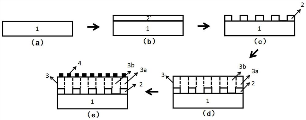
[0048] The present invention also provides a method for preparing a self-driven MSM ultraviolet detector, comprising the following steps:

[0049] a) depositing a low-temperature crystalline layer raw material on the surface of the substrate to obtain a low-temperature crystalline layer;

[0050] The material of the low-temperature crystalline layer is nitride of wurtzite structure; the deposition temperature is 300-950°C;

[0051] b) performing a patterning process on the low-temperature crystal layer to obtain a substrate with a patterned low-temperature crystal layer on the surface;

[0052] c) performing high temperature epitaxial growth on the surface of the substrate obtained in step b) to obtain a high temperature epitaxial layer;

[0053] The material of the high-temperature epitaxial layer is a nitride of wurtzite structure, and the temperature of the high-temperature epitaxial growth is 1000-1200° C.;

[0054] The high-temperature epitaxial layer epitaxially obtain...

Embodiment 1

[0069] To prepare a self-driven MSM UV detector, the specific steps are as follows:

[0070] a) A 20nm AlN low temperature crystalline layer was deposited on a 2-inch flat sapphire based on MOCVD technology; wherein, the deposition temperature of the crystalline layer was 850°C, the deposition pressure was 150torr, and the aluminum source used for the deposition was trimethylaluminum (TMA). ), the nitrogen source is ammonia (NH 3 ).

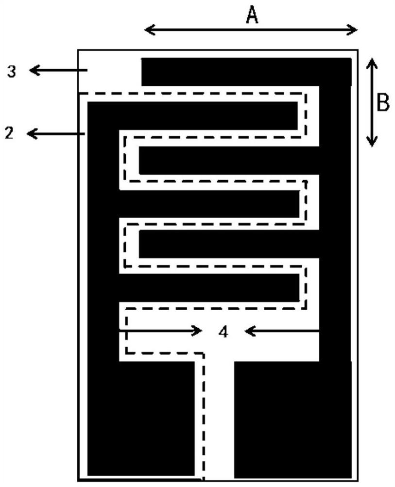
[0071] b) Spin-coat 1.5 μm thick photoresist on the surface of the substrate deposited with the low-temperature crystalline layer, use a contact exposure apparatus to expose and develop, and form an interdigitated patterned structure on the photoresist layer; wherein, the exposure time is 8 seconds, the development time is 30 seconds; the interdigital structure period values ​​are 16 and 24 microns, respectively, and the length is 500 microns.

[0072] c) Based on plasma etching, remove the AlN low temperature crystalline layer of the exposed p...

Embodiment 2

[0078] a) A 50nm AlN low-temperature crystalline layer was deposited on a 2-inch flat sapphire based on magnetron sputtering technology; wherein, the deposition temperature of the crystalline layer was 400°C, and the deposition pressure was 3×10 -5 Pa, the aluminum source used for deposition is metal aluminum target, and the nitrogen source is nitrogen (N 2 ).

[0079]b) patterning the surface of the sapphire substrate deposited with the AlN low temperature crystalline layer by step exposure technology to form an interdigitated patterned structure; wherein the interdigitated structure has a period value of 16 microns and a length of 500 microns.

[0080] c) depositing a Ti etching barrier layer with a thickness of 50 nm; etching the lower AlN low-temperature crystalline layer based on wet etching technology; wherein, the etchant used is 3 mol / L KOH aqueous solution, and the etching temperature is 70°C; after the etching, use deionized water to clean the sample, and then use H...


PUM

PropertyMeasurementUnit
thicknessaaaaaaaaaa
thicknessaaaaaaaaaa
thicknessaaaaaaaaaa

Abstract

The invention belongs to the technical field of semiconductor photoelectric devices, and particularly relates to a self-driven MSM ultraviolet detector and a preparation method thereof. The ultraviolet detector provided by the invention comprises a substrate; the patterned low-temperature crystallization layer is arranged on the surface of the substrate; the high-temperature epitaxial layer is arranged on the surface of the patterned low-temperature crystallization layer and an area, not covered with the patterned low-temperature crystallization layer, of the surface of the substrate; the high-temperature epitaxial layer arranged on the patterned low-temperature crystallization layer has metal polarity, and the high-temperature epitaxial layer arranged on the area, not covered with the patterned low-temperature crystallization layer, of the surface of the substrate has nitrogen polarity; the interdigital electrode is arranged on the high-temperature epitaxial layer; the interdigital electrode is composed of two groups of electrodes, one group of electrodes is arranged in a metal polarity area of the high-temperature epitaxial layer, and the other group of electrodes is arranged in a nitrogen polarity area of the high-temperature epitaxial layer. According to the MSM ultraviolet detector provided by the invention, the responsivity and the overall performance of the detector are remarkably improved under a simple framework of an MSM structure, so that the MSM ultraviolet detector can perform self-driven detection.

Description

technical field [0001] The invention belongs to the technical field of semiconductor optoelectronic devices, in particular to a self-driven MSM ultraviolet detector and a preparation method thereof. Background technique [0002] Ultraviolet detection technology complements infrared and laser detection technology. It is a photoelectric detection technology that has received extensive attention in recent years. It has extremely important applications in ultraviolet early warning and reconnaissance, ultraviolet communication, fire alarm system, environmental pollution monitoring, medical imaging and other fields. The most common ultraviolet detectors in the field are mainly Si-based photodiodes. However, due to the narrow band gap of Si, a filter system must be used to filter out visible light waves, thereby realizing the detection of ultraviolet light. In contrast, UV detectors based on wide-bandgap semiconductor materials such as GaN and AlGaN can directly detect UV light. T...

Claims


Application Information

Patent Timeline
Patent Type & Authority Applications(China)
IPC IPC(8): H01L31/108H01L31/0224H01L31/18
CPCH01L31/1085H01L31/1856H01L31/1852H01L31/022408Y02P70/50
Inventor 郭炜国琛雨陈荔叶继春
Owner NINGBO INST OF MATERIALS TECH & ENG CHINESE ACADEMY OF SCI
Why Eureka
Try Eureka