Silicon carbide single crystal wafer, silicon carbide crystal, preparation method and semiconductor device

A silicon carbide single crystal, silicon carbide technology, applied in semiconductor devices, semiconductor/solid-state device manufacturing, chemical instruments and methods, etc., can solve the problems of reducing dislocation density and not improving device yield.

Active Publication Date: 2022-05-27
BEIJING TIANKE HEDA SEMICON CO LTD +3
View PDF4 Cites 2 Cited by
  • Summary
  • Abstract
  • Description
  • Claims
  • Application Information

AI Technical Summary

Problems solved by technology

[0004] In view of this, the present invention provides a silicon carbide single wafer and its preparation method, a silicon carbide crystal and its preparation method, and a semiconductor device to solve the problem that the dislocation density has been reduced in the prior art, but the device yield has not been improved.

Method used


Image

  • Silicon carbide single crystal wafer, silicon carbide crystal, preparation method and semiconductor device
  • Silicon carbide single crystal wafer, silicon carbide crystal, preparation method and semiconductor device
  • Silicon carbide single crystal wafer, silicon carbide crystal, preparation method and semiconductor device

Examples


preparation example Construction

[0084] In addition, an embodiment of the present invention also provides a method for preparing a silicon carbide crystal, please refer to Figure 12 , Figure 12 A flow chart of a method for preparing silicon carbide crystals provided in an embodiment of the present invention; the method for preparing silicon carbide crystals includes:

[0085] S101: pretreating the crucible containing the silicon carbide raw material with a graphite cover without a seed crystal;

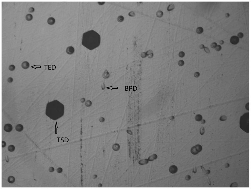
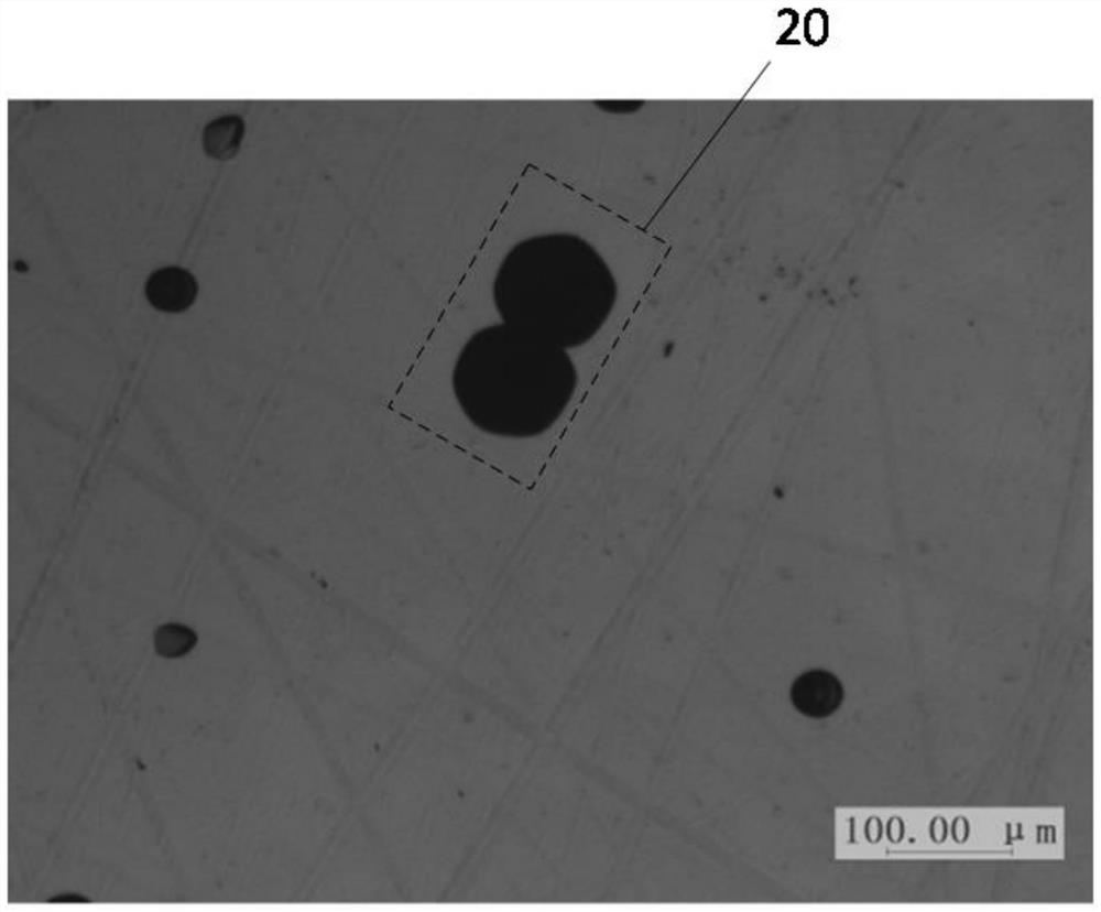
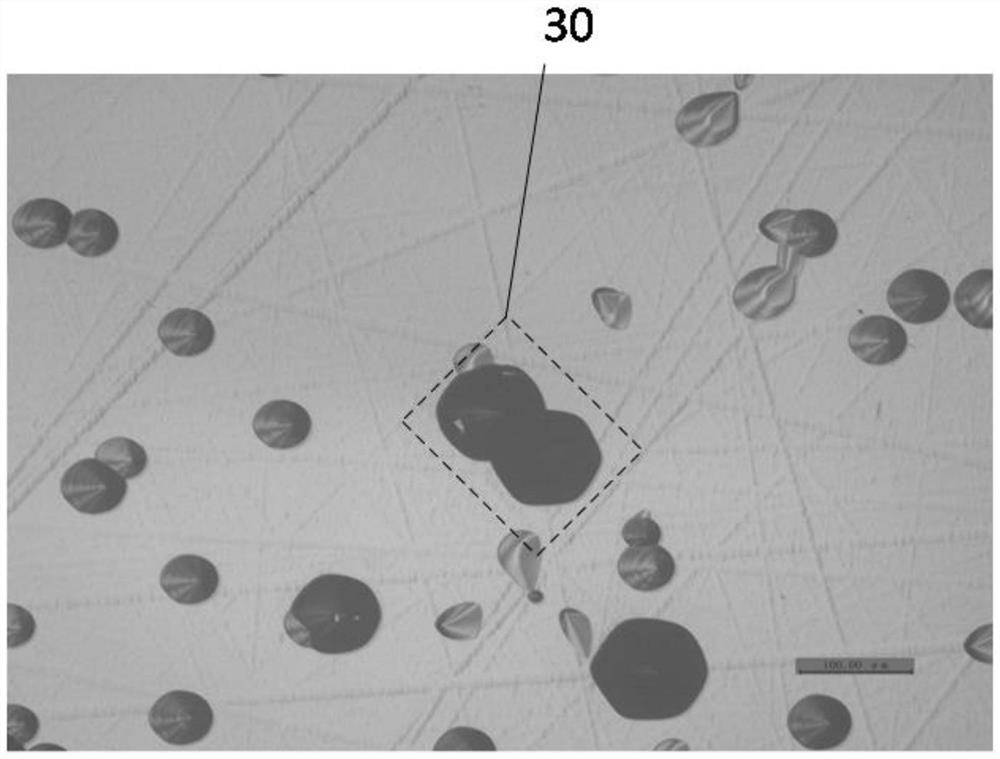
[0086] It should be noted that in the initial stage of silicon carbide growth, various defects such as carbon inclusions and polytypes will occur at the extension interface. Through a large number of mechanism research and analysis, the inventor found that it is easy to form aggregated screw dislocations at the defect positions of the inclusions, and polytype defects. It will lead to aggregated basal plane dislocations, aggregated edge dislocations, etc.

[0087] Through a lot of experimental research, the invent...

Embodiment 1

[0106]Example 1——The crucible containing the silicon carbide raw material is added with a graphite cover without seed crystal, and is loaded into the silicon carbide single crystal furnace, and the high temperature is 2200 degrees, and the pressure is lower than 0.1Pa, and the vacuum pump is turned on all the time. After 5 hours, the furnace was stopped and cooled, and the crucible containing the silicon carbide raw material was weighed. It was found that the weight decreased by 3%, indicating that the impurities on the raw material and the surface of the crucible, and the silicon-rich components have been effectively disposed of.

[0107] Select a 4-degree 6-inch seed crystal of a SiC sheet with low aggregate dislocation density, and fix the seed crystal to the lid. Replace a graphite cover without a seed crystal, install a cover with a seed crystal, and re-install the furnace for growth after assembly. The temperature is 2300 degrees, the fluctuation is less than 1 degree, th...


PUM


Abstract

The invention provides a silicon carbide single crystal wafer and a preparation method thereof, a silicon carbide crystal and a preparation method thereof, and a semiconductor device, the surface of the silicon carbide single crystal wafer is the surface of which the normal direction and the c direction form an included angle of 0-8 degrees, the aggregation dislocation on the silicon carbide single crystal wafer is less than 300/cm < 2 >, and the aggregation dislocation refers to that after molten KOH corrosion, the surface of the silicon carbide single crystal wafer is subjected to thermal treatment. In the obtained corrosion pits, the distance between the geometric centers of any two corrosion pits is less than 80 microns. Even if the dislocation density is relatively high, the aggregation dislocation density is also relatively low, so that the yield of the silicon carbide-based device is improved.

Description

technical field [0001] The invention relates to the technical field of semiconductor materials, in particular to a silicon carbide single wafer and a preparation method thereof, a silicon carbide crystal and a preparation method thereof, and a semiconductor device. Background technique [0002] In the prior art, dislocation is one of the main defects of a single silicon carbide wafer; it has a significant impact on the performance of silicon carbide devices. At present, the dislocation density of products on the market is still relatively high. In recent years, with technological progress, the dislocation density has gradually decreased , but still does not meet the requirements. [0003] Moreover, the inventors found that even if the dislocation density of the wafer is reduced, the device yield cannot sometimes be improved, and the correlation between dislocations and device failures is still largely unknown. SUMMARY OF THE INVENTION [0004] In view of this, the present...

Claims


Application Information

Patent Timeline
Patent Type & Authority Applications(China)
IPC IPC(8): C30B29/36C30B1/12C30B33/02H01L29/04H01L29/16H01L29/34
CPCC30B29/36C30B1/12C30B33/02H01L29/045H01L29/1608H01L29/34C30B23/00C01B32/956C01P2006/10C30B23/02
Inventor 刘春俊娄艳芳彭同华王波赵宁郭钰杨建张平邹宇杨帆
Owner BEIJING TIANKE HEDA SEMICON CO LTD
Why Eureka
Try Eureka