Silicon wafer, silicon wafer textured structure and preparation method of silicon wafer textured structure
A silicon wafer and suede technology, applied in the direction of semiconductor devices, electrical components, circuits, etc., can solve the problems of low fill factor, deformation of screen printing graphics, misalignment, etc., to overcome the low fill factor , It is beneficial to the printing alignment and the effect of increasing the surface area
- Summary
- Abstract
- Description
- Claims
- Application Information
AI Technical Summary
Problems solved by technology
Method used
Image

Examples
Embodiment 1
[0065] This embodiment provides a preparation method of a silicon wafer textured structure, and the preparation method includes the following steps:
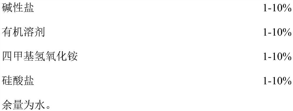
[0066] (1) Under the condition of 70°C, the silicon wafer is subjected to anisotropic alkaline texturing treatment in alkaline solution for 400s, and the first silicon wafer is obtained after drying; in terms of mass percentage, the alkaline solution includes: 5% alkaline solution salt, 5% organic solvent, 5% tetramethylammonium hydroxide, 5% silicate, and the balance is water; the basic salt is potassium hydroxide, the organic solvent is isopropanol, so The silicate is sodium silicate;
[0067] (2) Screen-printing nanometer metal particle slurry in the electrode setting area of the first silicon wafer obtained in step (1), and drying at 120° C. to obtain a second silicon wafer with a slurry layer thickness of 50 nm; The metal particle slurry is composed of water-soluble gold nanoparticles with a mass ratio of 70:3:20, an org...
Embodiment 2
[0071] This embodiment provides a preparation method of a silicon wafer textured structure, and the preparation method includes the following steps:
[0072] (1) Under the condition of 60°C, anisotropic alkali texturing treatment is performed on the silicon wafer in alkaline solution for 500s, and the first silicon wafer is obtained after drying; in terms of mass percentage, the alkaline solution includes: 3% alkaline solution salt, 3% organic solvent, 8% tetramethylammonium hydroxide, 8% silicate, the balance is water; the basic salt is sodium hydroxide, the organic solvent is absolute ethanol, so The silicate is potassium silicate;
[0073] (2) Screen-printing nanometer metal particle slurry in the electrode setting area of the first silicon wafer obtained in step (1), and drying at 80°C to obtain a second silicon wafer with a slurry layer thickness of 40 nm; The metal particle slurry is composed of water-soluble nano silver particles with a mass ratio of 80:2:15, an orga...
Embodiment 3
[0077] This embodiment provides a preparation method of a silicon wafer textured structure, and the preparation method includes the following steps:
[0078] (1) Under the condition of 80°C, anisotropic alkali texturing treatment is performed on the silicon wafer in alkaline solution for 300s, and the first silicon wafer is obtained after drying; in terms of mass percentage, the alkaline solution includes: 8% alkaline Salt, 8% organic solvent, 3% tetramethylammonium hydroxide, 3% silicate, the balance is water; the basic salt is potassium hydroxide, the organic solvent is absolute ethanol, so The silicate is sodium silicate;
[0079](2) Screen-printing nano-metal particle paste in the electrode setting area of the first silicon wafer obtained in step (1), and drying at 160° C. to obtain a second silicon wafer with a paste layer thickness of 80 nm; The metal particle slurry is composed of water-soluble nano-copper particles with a mass ratio of 60:4:25, an organic binder and...
PUM
| Property | Measurement | Unit |
|---|---|---|
| The average particle size | aaaaa | aaaaa |
| The average particle size | aaaaa | aaaaa |
| The average particle size | aaaaa | aaaaa |
Abstract
Description
Claims
Application Information
 - Generate Ideas
- Intellectual Property
- Life Sciences
- Materials
- Tech Scout
- Unparalleled Data Quality
- Higher Quality Content
- 60% Fewer Hallucinations
Browse by: Latest US Patents, China's latest patents, Technical Efficacy Thesaurus, Application Domain, Technology Topic, Popular Technical Reports.
© 2025 PatSnap. All rights reserved.Legal|Privacy policy|Modern Slavery Act Transparency Statement|Sitemap|About US| Contact US: help@patsnap.com