Feed network system

A technology of feed network and network, applied in the field of feed network system, can solve the problems of obvious dispersion effect of phase shifting line, long processing cycle, inconsistent sintering shrinkage rate of substrate and slurry, etc., and achieves wide application value and applicability technology Effect, thermal performance and mechanical performance guarantee, the effect of good electromagnetic shielding effect

Pending Publication Date: 2022-07-12
NO 54 INST OF CHINA ELECTRONICS SCI & TECH GRP
View PDF0 Cites 0 Cited by
  • Summary
  • Abstract
  • Description
  • Claims
  • Application Information

AI Technical Summary

Problems solved by technology

[0002] At present, the feed network mostly adopts the form of a power combiner plus a phase-shifting line, and the dispersion effect of the phase-shifting line is obvious. The influence of the phase-shifting line on the phase is only for a certain frequency point or a very narrow bandwidth, and the structure is not symmetrical and unified. , poor reconfigurability
[0003] The current LTCC and HTCC processes are complex, layer by layer, and there are many difficulties in design reliability. The shrinkage rate and thermal expansion coefficient when the substrate and wiring are co-fired are one of the important challenges, which are mainly reflected in three aspects: sintering density The sintering shrinkage rate of the substrate and the slurry is inconsistent; the sintering densification speed does not match. These mismatches can easily lead to uneven, warped, and delaminated substrate surfaces after firing. Another consequence of the mismatch is metal wiring. decrease in adhesion
LTCC substrates are fragile and have low thermal conductivity, heat dissipation is still a key issue, and the processing cycle is long and expensive, which is not convenient for large-scale production in a short cycle
[0004] At present, in the stripline antenna feeding network manufactured by the multilayer microwave printed board, the processing is simple, the material microstructure is uniform, low dielectric constant and low loss can be achieved, and the thermal and mechanical properties are guaranteed. The application of double-sided blind hole technology is less, resulting in poor electromagnetic shielding effect and affecting the transmission of signals between multi-layer boards, and most of them are one-layer planar structure with large size, which is not conducive to the development of miniaturization
[0005] In 2021, Southeast University disclosed a phased array antenna feeding network, which is realized by high-density multi-layer mixed laminated board, but only has single-sided blind hole processing technology, and has not realized double-sided blind hole and buried hole technology.
[0006] In the PCB processing process, the distance between the ground hole and the edge of the buried resistor must be at least 500um, so as to ensure that the drilling will not be biased to the buried resistor, so that the design of the multilayer microwave printed board is limited by the processing accuracy.

Method used


Image

  • Feed network system
  • Feed network system
  • Feed network system

Examples


Embodiment Construction

[0040] Hereinafter, the present invention will be further described with reference to the accompanying drawings and specific embodiments.

[0041] In order to illustrate the technical solutions of the embodiments of the present invention more clearly, the accompanying drawings of the embodiments will be briefly introduced below. Obviously, the drawings in the following description are only some embodiments of the present invention, which will be useful to those skilled in the art. In other words, on the premise of no creative work, other drawings can also be obtained from these drawings.

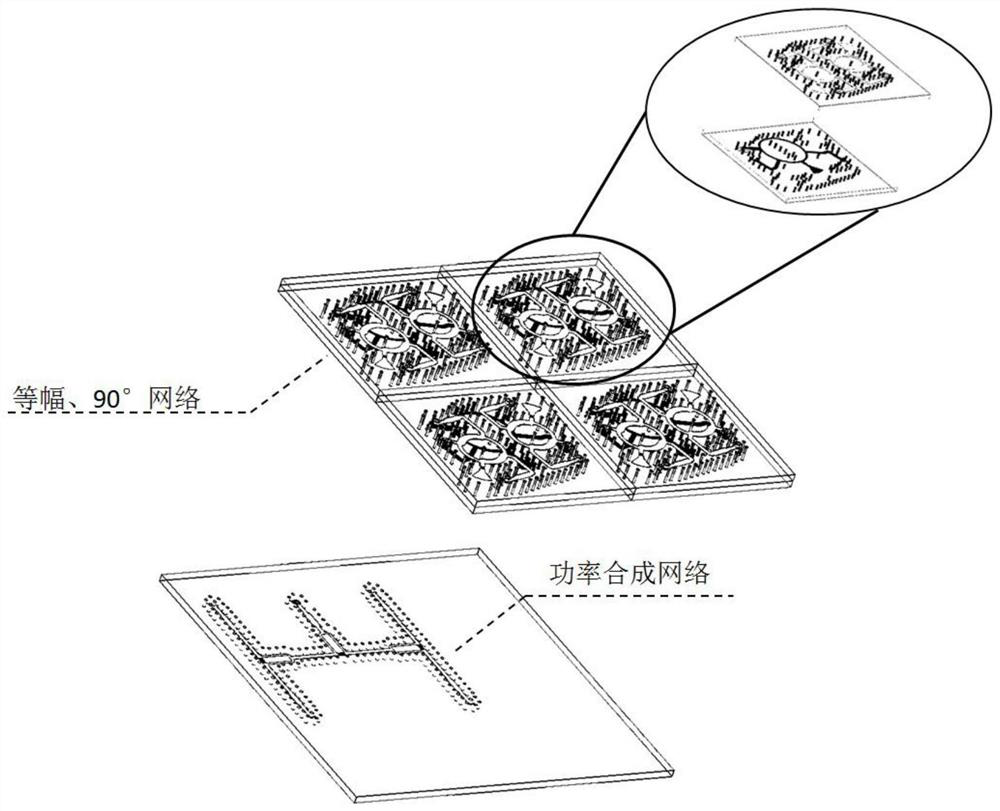
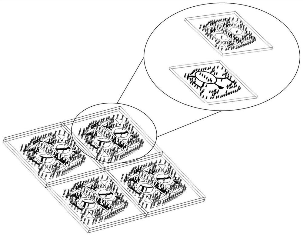
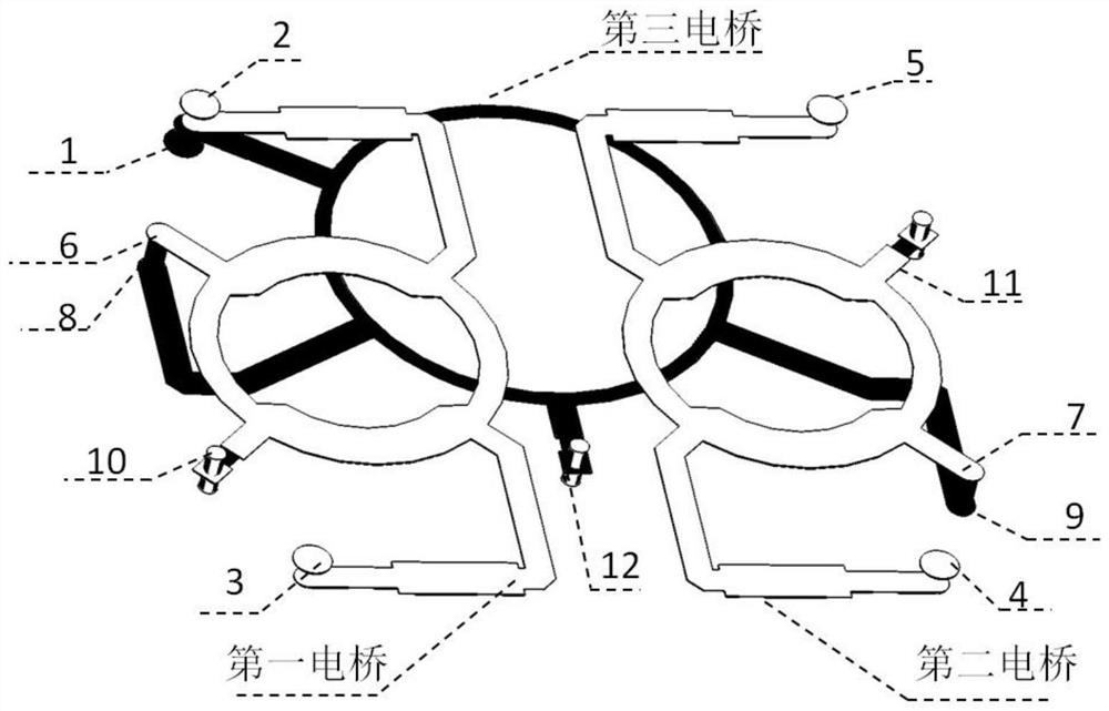
[0042] This embodiment is an antenna feeding network system based on the multi-layer mixed-voltage buried resistance technology and the high-density vertical interconnection technology PCB process: including a first electric bridge, a second electric bridge and a third electric bridge connected to each other to form upper and lower layers, etc. A transmission network and a four-in-one Wilkin...


PUM


Abstract

The invention discloses a feed network system, and belongs to the technical field of antenna feed. The antenna comprises four equal-amplitude 90-degree network sub-arrays of 2 * 2 rectangular arrays and a power synthesis network which is located at the bottoms of the sub-arrays and composed of four-in-one Wilkinson power synthesizers. The equal-amplitude 90-degree network sub-arrays of the four arrays realize signal synthesis output through a cascaded four-in-one Wilkinson power combiner; the equal-amplitude 90-degree network subarray comprises a first metal grounding plate, a first microwave substrate, a first metal signal line, a first prepreg, a second microwave substrate, a second metal grounding plate, a second prepreg, a second metal signal line, a third microwave substrate and a third metal grounding plate which are sequentially stacked from top to bottom; the microwave substrates are bonded through prepregs; and a feed network capable of butting four-feed-point right-handed rotation equal-amplitude 90-degree antenna signals is realized. According to the invention, the horizontal transverse size of the feed network is reduced, and miniaturization and high integration of the antenna array are realized.

Description

technical field [0001] The invention relates to the technical field of antenna feeding, in particular to a feeding network system suitable for high-density vertical interconnection technology PCB. Background technique [0002] At present, the feed network mostly adopts the form of power combiner and phase-shifting line, and the dispersion effect of the phase-shifting line is obvious. The influence of the phase-shifting line on the phase is only for a certain frequency point or within a very narrow bandwidth, and the structure is not symmetrical and uniform. , the reconfigurability is poor. [0003] The current LTCC and HTCC processes are complex, layer by layer, and there are many difficulties in design reliability. The shrinkage rate and thermal expansion coefficient when the substrate and wiring are co-fired are one of the important challenges, which are mainly reflected in three aspects: dense sintering Inconsistent finishing temperature; inconsistent sintering shrinkage...

Claims


Application Information

Patent Timeline
Patent Type & Authority Applications(China)
IPC IPC(8): H01Q21/00H01Q1/48H01Q1/50H01Q1/52H01Q3/34
CPCH01Q21/0075H01Q1/48H01Q1/50H01Q1/526H01Q3/34H01Q1/52
Inventor 刘子奕魏浩韩威杨文涛赵建欣魏恒赵琪
Owner NO 54 INST OF CHINA ELECTRONICS SCI & TECH GRP
Why Eureka
Try Eureka