GaN-based light emitting diode epitaxial wafer and preparation method thereof

A technology of light-emitting diodes and epitaxial wafers, applied in chemical instruments and methods, crystal growth, polycrystalline material growth, etc., can solve problems affecting the luminous efficiency of light-emitting diodes, affecting the luminous brightness of light-emitting diodes, serious In segregation, etc., to improve the interface Effects of crystal quality, crystal quality improvement, and defect reduction

Pending Publication Date: 2022-07-26
JIANGXI ZHAO CHI SEMICON CO LTD
View PDF0 Cites 4 Cited by
  • Summary
  • Abstract
  • Description
  • Claims
  • Application Information

AI Technical Summary

Problems solved by technology

However, the low temperature will make the cracking of ammonia insufficient, resulting in defects such as N vacancies, resulting in more defects at the interface of the quantum well barrier, making the segregation of In more serious, affecting the luminous efficiency of the light-emitting diode, and then affecting the luminous brightness of the light-emitting diode

Method used


Image

  • GaN-based light emitting diode epitaxial wafer and preparation method thereof
  • GaN-based light emitting diode epitaxial wafer and preparation method thereof
  • GaN-based light emitting diode epitaxial wafer and preparation method thereof

Examples


Embodiment 1

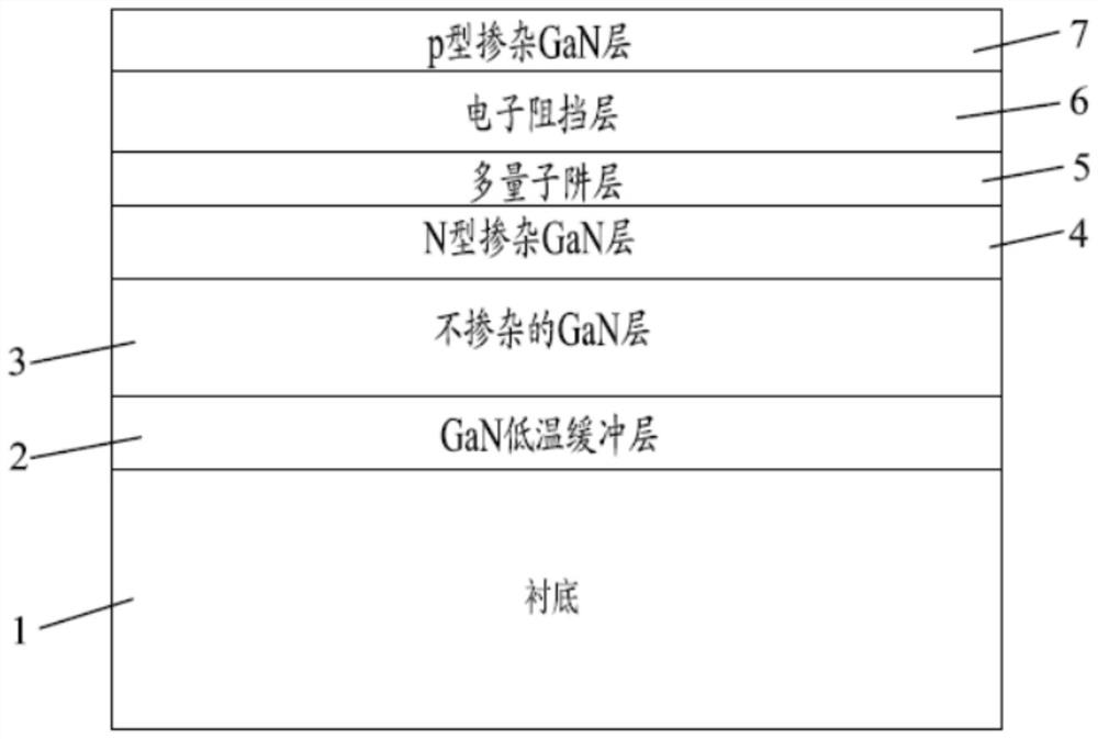
[0036] see Figure 1-Figure 3 , shows the GaN-based light-emitting diode epitaxial wafer in the first embodiment of the present invention, including a substrate 1, and a GaN low-temperature buffer layer 2 epitaxially grown on the substrate 1 in turn, an undoped GaN layer 3, and an N-type doped GaN layer. Hetero GaN layer 4 , multiple quantum well layer 5 , electron blocking layer 6 and p-type doped GaN layer 7 .

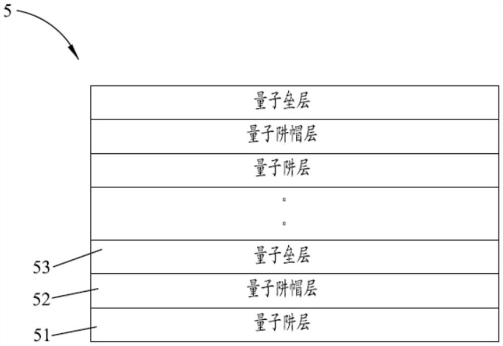
[0037] In this embodiment, as figure 2 As shown, the multiple quantum well layer 5 is a periodic structure in which quantum well layers 51 , quantum well cap layers 52 and quantum barrier layers 53 are alternately stacked. The quantum well layer 51 may be an InGaN quantum well layer, and the quantum barrier layer 53 may be a GaN quantum barrier layer. The quantum well cap layer 52 is inserted between the quantum well layer 51 and the quantum barrier layer 53, and is mainly used for the purpose of protecting the In composition of the quantum well and reducing the l...

Embodiment 2

[0058] The second embodiment of the present invention also provides a GaN-based light-emitting diode epitaxial wafer and a preparation method thereof. The GaN-based light-emitting diode epitaxial wafer and its preparation method in this embodiment are the same as the GaN-based light-emitting diode epitaxial wafer and its preparation in the first embodiment. The methods differ in that:

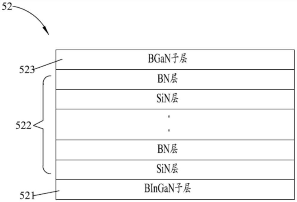
[0059] The BInGaN sublayer still does not pass H during the growth 2 , the H introduced during the growth of the composite sublayer 2 The amount is 2L, and the H introduced during the growth of the BGaN sublayer 2 The volume is 8L.

Embodiment 3

[0061] The third embodiment of the present invention also provides a GaN-based light-emitting diode epitaxial wafer and a preparation method thereof. The GaN-based light-emitting diode epitaxial wafer and its preparation method in this embodiment are the same as the GaN-based light-emitting diode epitaxial wafer and its preparation in the first embodiment. The methods differ in that:

[0062] The BInGaN sublayer still does not pass H during the growth 2 , the H introduced during the growth of the composite sublayer 2 The amount is 3L, and the H introduced during the growth of the BGaN sublayer 2 The volume is 10L.


PUM

PropertyMeasurementUnit
temperatureaaaaaaaaaa
thicknessaaaaaaaaaa
thicknessaaaaaaaaaa

Abstract

The invention provides a GaN-based light-emitting diode epitaxial wafer and a preparation method thereof, the GaN-based light-emitting diode epitaxial wafer comprises a multi-quantum well layer, and the multi-quantum well layer is of a periodic structure formed by alternately stacking quantum well layers, quantum well cap layers and quantum barrier layers; the quantum well cap layer comprises a BInGaN sub-layer, a composite sub-layer and a BGaN sub-layer which are stacked in sequence, the composite sub-layer is of a periodic structure formed by alternately stacking SiN layers and BN layers, the growth temperature gradient of the BInGaN sub-layer, the growth temperature gradient of the composite sub-layer and the growth temperature gradient of the BGaN sub-layer are increased, and the In component content of the BInGaN sub-layer is gradually reduced. The cap layer in the multi-quantum well layer is specially designed, so that the aim of protecting the In component of the quantum well is well fulfilled, well-barrier lattice mismatch is reduced, In segregation at a quantum well-barrier interface is relieved, the interface crystal quality at the quantum well-barrier is improved, the well-barrier interface is steeper, and the performance of the device is improved. The improvement of wavelength uniformity and the acquisition of better antistatic capability are facilitated, and the luminous efficiency of the light-emitting diode is successfully improved.

Description

technical field [0001] The invention relates to the technical field of light-emitting diodes, in particular to a GaN-based light-emitting diode epitaxial wafer and a preparation method thereof. Background technique [0002] At this stage, GaN-based light-emitting diodes (Light Emitting Diodes, LEDs for short) have been widely used due to their advantages of high efficiency, energy saving, and environmental protection. As the core region of blue-green light-emitting diodes, the multiple quantum well structure has been widely studied. Multiple quantum wells are generally formed by alternately stacking InGaN quantum well layers and GaN quantum barrier layers. However, due to the mismatch of lattice constants between the InGaN quantum well layer and the GaN quantum barrier layer, many defects are generated at the interface of the quantum well barrier. Excessive defects in multiple quantum wells will cause In segregation, and the non-radiative review will increase greatly, thus...

Claims


Application Information

Patent Timeline
Patent Type & Authority Applications(China)
IPC IPC(8): H01L33/06C30B25/18C30B29/40C30B29/68H01L33/00H01L33/14H01L33/32
CPCH01L33/06H01L33/145H01L33/325H01L33/0075C30B25/183C30B29/403C30B29/406C30B29/68
Inventor 张彩霞程金连印从飞胡加辉金从龙
Owner JIANGXI ZHAO CHI SEMICON CO LTD
Why Eureka
Try Eureka