
Metal organic framework material semiconductor crystal and preparation method and application thereof

A metal-organic framework and semiconductor technology, which is applied in the field of metal-organic framework material semiconductor crystals and their preparation, can solve the problems of unadjustable structure and function, poor performance, insufficient types of semiconductors, etc., so as to achieve mass production and reduce production costs. , The effect of excellent X-ray direct detection performance

Active Publication Date: 2022-07-29
MINDU INNOVATION LAB +1
View PDF5 Cites 1 Cited by
  • Summary
  • Abstract
  • Description
  • Claims
  • Application Information

AI Technical Summary

Problems solved by technology

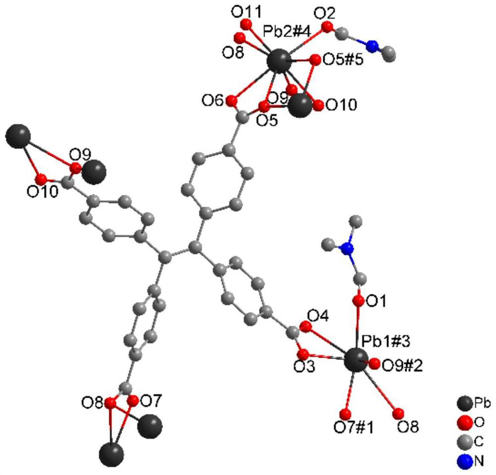
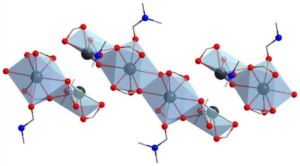
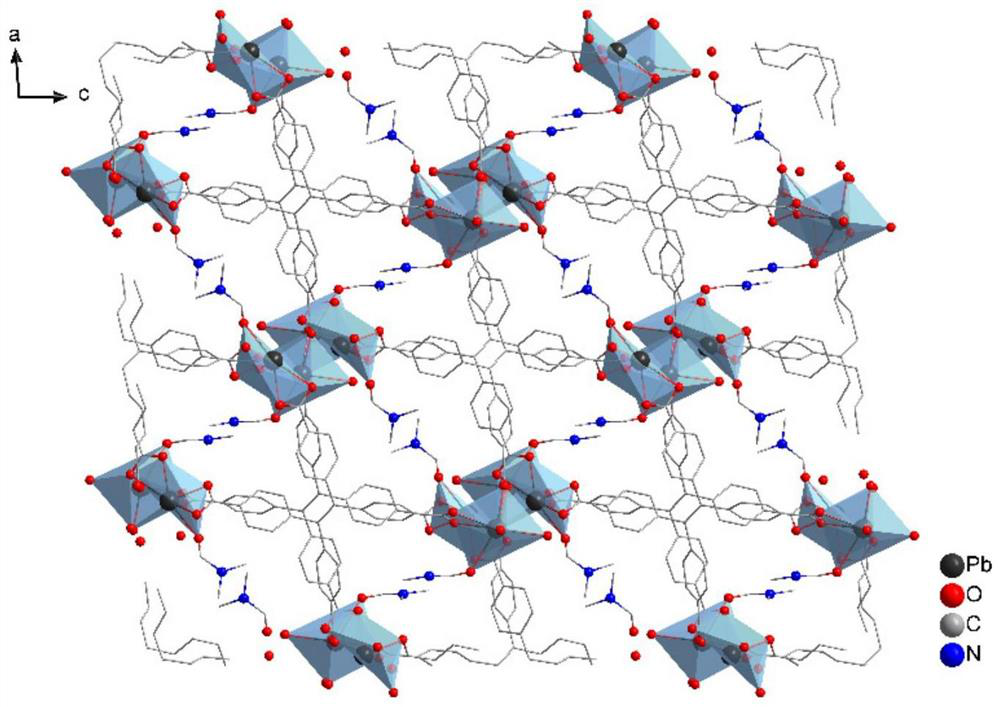
[0004] The object of the present invention is that, in order to overcome the problems of insufficient semiconductor types, poor performance, and unadjustable structure and function in the field of ray detection in the prior art, a lead-based metal-organic framework Pb is synthesized by a solvothermal method. 2 (TCPE)(DMF) 2 ·H 2 O(Pb-TCPE), Pb-TCPE is a new type of semiconductor material, which has a large atomic number of Pb 2+ and redox-active large conjugated organic ligands, the constructed semiconductors provide favorable internal structural conditions for X-ray absorption, conversion, and charge transport.

Method used


Image

  • Metal organic framework material semiconductor crystal and preparation method and application thereof
  • Metal organic framework material semiconductor crystal and preparation method and application thereof
  • Metal organic framework material semiconductor crystal and preparation method and application thereof

Examples


Embodiment 1

[0044] The weighed PbCl 2 (33.4 mg, 0.12 mmol) and H 4TCPE (30.5 mg, 0.06 mmol) was added to 6 mL of a mixed solvent of N,N-dimethylformamide (DMF) and deionized water (5:1, V / V), and the resulting mixed solution was sealed in a 20 mL glass bottle And sonicated in an ultrasonic cleaner for 10 minutes to thoroughly mix the reaction raw materials. Then, the glass vial was put into a temperature-controlled drying oven and slowly heated to 100° C., kept at 100° C. for 72 h, and then naturally cooled to room temperature. The colorless and transparent flaky crystals of Pb-TCPE were obtained, which were collected and washed with DMF for several times, and finally dried in an oven at 65 °C for 6 h.

Embodiment 2

[0046] The weighed PbCl 2 (33.4 mg, 0.12 mmol) and H 4 TCPE (30.5 mg, 0.06 mmol) was added to 6 mL of a mixed solvent of N,N-dimethylformamide (DMF) and deionized water (5:1, V / V), and the resulting mixed solution was sealed in a 20 mL glass bottle And sonicated in an ultrasonic cleaner for 10 minutes to thoroughly mix the reaction raw materials. Then, the glass vial was put into a temperature-controlled drying oven and slowly heated to 90° C., kept at 90° C. for 60 h, and then naturally cooled to room temperature. The colorless and transparent flaky crystals of Pb-TCPE were obtained, which were collected and washed with DMF for several times, and finally dried in an oven at 65 °C for 6 h.

Embodiment 3

[0048] The weighed PbCl 2 (16.7 mg, 0.06 mmol) and H 4 TCPE (30.5 mg, 0.06 mmol) was added to 6 mL of a mixed solvent of N,N-dimethylformamide (DMF) and deionized water (5:1, V / V), and the resulting mixed solution was sealed in a 20 mL glass bottle And sonicated in an ultrasonic cleaner for 10 minutes to thoroughly mix the reaction raw materials. Then, the glass vial was put into a temperature-controlled drying oven and slowly heated to 100° C., kept at 100° C. for 72 h, and then naturally cooled to room temperature. The colorless and transparent flaky crystals of Pb-TCPE were obtained, which were collected and washed with DMF for several times, and finally dried in an oven at 65 °C for 6 h.


PUM

PropertyMeasurementUnit
Sensitivityaaaaaaaaaa

Abstract

The invention discloses a metal organic framework material semiconductor crystal, the chemical formula of the semiconductor crystal is C36H32N2O11Pb2, and the molecular structural formula of the semiconductor crystal is Pb2 (TCPE) (DMF) 2. H2O, the semiconductor single crystal obtained by the method disclosed by the invention crystallizes in a P21 / n space group of a monoclinic system, and the shape of the semiconductor single crystal is a micron-scale lamellar crystal. The material has good X-ray direct detection performance, the detection sensitivity reaches up to 4812.6 [mu] C Gyair <-1 >. Cm <-2 > under the bias voltage of 50V, the lowest detection limit is 0.09329 [mu] Gyair / s under the bias voltage of 20V, and the material can be used as an excellent candidate material of a novel radiation detection semiconductor.

Description

technical field [0001] The application belongs to the technical field of semiconductor crystal material preparation, and in particular relates to a metal organic framework material semiconductor crystal and a preparation method and application thereof. Background technique [0002] The detection of high-energy rays (X-rays, γ-rays, etc.) is an important research direction in recent years, and it plays an extremely important role in the fields of national security, medical treatment and multidisciplinary research. For X-ray detection, there are usually two strategies of indirect detection and direct detection. Compared with the indirect detection strategy of converting X-rays into ultraviolet and visible light, and then collecting and converting them into electrical signals by photomultiplier tubes, direct detection directly converts X-rays into electrical signals, reducing the signal loss of secondary conversion and the interference between photons. Optical crosstalk. It h...

Claims


Application Information

Patent Timeline
Patent Type & Authority Applications(China)
IPC IPC(8): C08G83/00
CPCC08G83/008Y02E10/549
Inventor 王帅华古奇吴少凡黄鑫郑熠
Owner MINDU INNOVATION LAB
Learn More