Unsealing method of plastic package copper bonding lead semiconductor device

A copper bonding and semiconductor technology, applied in the field of unsealing of electronic components, can solve problems such as inability to accurately grasp the speed, long unsealing time, and poor unsealing effect

Pending Publication Date: 2022-07-29
北京京瀚禹电子工程技术有限公司
View PDF0 Cites 2 Cited by
  • Summary
  • Abstract
  • Description
  • Claims
  • Application Information

AI Technical Summary

Problems solved by technology

[0004] (1) Add CuSO to concentrated acid 4 ·5H 2 O crystals, using Cu 2+ The saturation effect can be unsealed, but the overall operation time of this method is relatively long, and it is not suitable for large-scale production
[0005] (2) The chemical electrolytic immersion method and the chemical low-temperature spray etching method are used for unsealing, but the chemical electrolytic immersion method requires a special device and the operation is more complicated; the chemical low-temperature spray etching method will fully contact the acid with the bonding wire, which is beneficial Copper bonding wires react with acid and take longer to unpack, less efficient for production
[0006] (3) Low temperature wet etching in pure nitrogen environment, the disadvantage of this method is that the cost is too high and the equipment requirements are very high
[0009] (1) The prior art ad

Method used


Image

  • Unsealing method of plastic package copper bonding lead semiconductor device
  • Unsealing method of plastic package copper bonding lead semiconductor device
  • Unsealing method of plastic package copper bonding lead semiconductor device

Examples


Embodiment Construction

[0046] In order to make the objectives, technical solutions and advantages of the present invention clearer, the present invention will be further described in detail below with reference to the embodiments. It should be understood that the specific embodiments described herein are only used to explain the present invention, but not to limit the present invention.

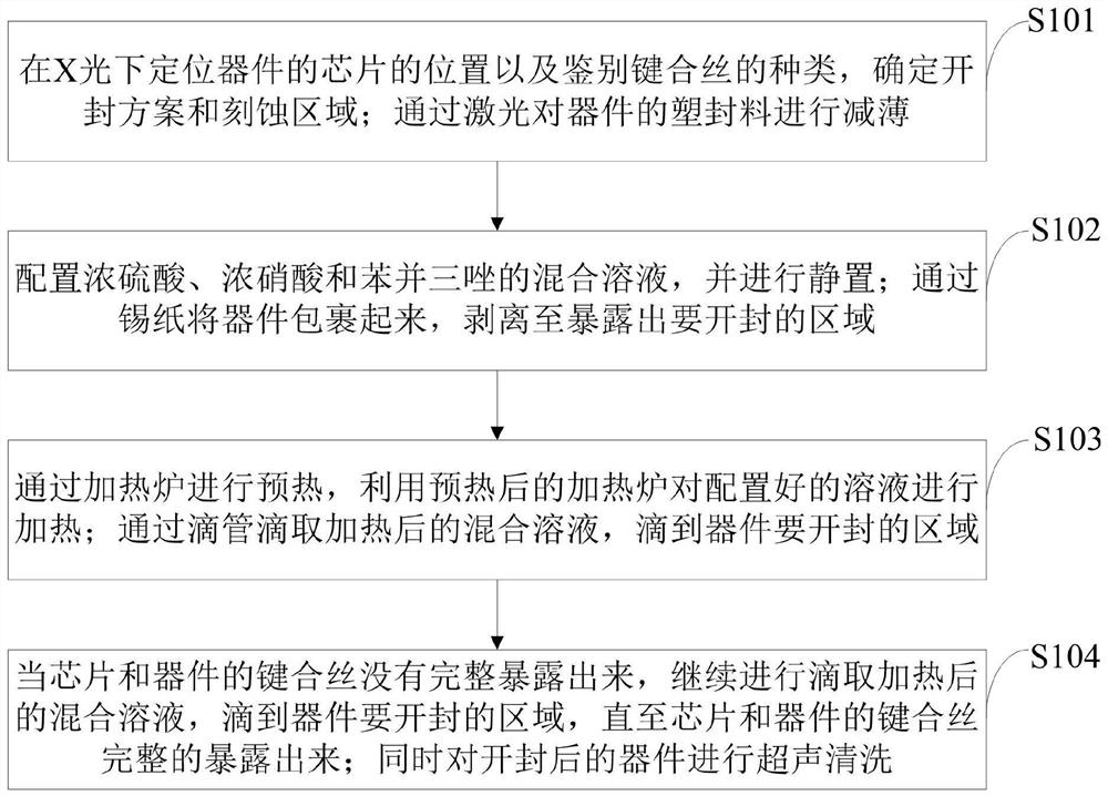
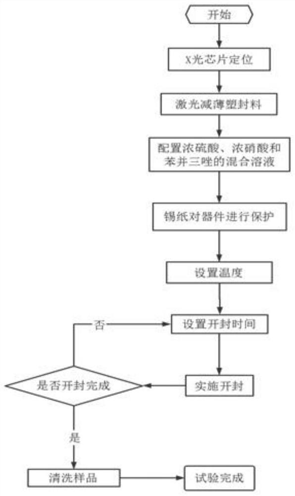
[0047] like figure 1 As shown, the method for unsealing a plastic-encapsulated copper-bonded wire semiconductor device provided by an embodiment of the present invention includes:

[0048]S101 : locate the position of the chip of the device and identify the type of bonding wire under X-ray, determine the unsealing plan and the etching area; thin the plastic sealing compound of the device by laser.

[0049] S102: Prepare a mixed solution of concentrated sulfuric acid, concentrated nitric acid and benzotriazole, and let it stand; wrap the device with tin foil, and peel it off to expose the area to be opened.

[005...


PUM


Abstract

The invention belongs to the technical field of unsealing of electronic components, and discloses an unsealing method of a plastic package copper bonding wire semiconductor device, which comprises the following steps: positioning the position of a chip of the device under X-ray, identifying the type of a bonding wire, and determining an unsealing scheme and an etching area; thinning a plastic package material of the device through laser; preparing a mixed solution of concentrated sulfuric acid, concentrated nitric acid and benzotriazole, and standing; wrapping the device by tinfoil, and stripping until an area to be unsealed is exposed; the preheated heating furnace is used for heating the prepared solution; dropwise taking the heated mixed solution through a dropper, and dropwise adding the mixed solution to a to-be-unsealed area of the device; when the bonding wires of the chip and the device are not completely exposed, continuously dripping the heated mixed solution to an unsealed area of the device until the bonding wires of the chip and the device are completely exposed; and carrying out ultrasonic cleaning on the unsealed device. The method is simple to operate, low in equipment requirement and high in test efficiency.

Description

technical field [0001] The invention belongs to the technical field of unsealing of electronic components, in particular to a method for unsealing a plastic-sealed copper bonding lead semiconductor device. Background technique [0002] At present, copper has good electrical conductivity, higher electrical conductivity than gold and aluminum, and its heat dissipation is significantly higher than that of gold and aluminum; in addition, copper has stable performance and is not easy to react with other metal compounds in the welding process; its higher The higher elongation and tensile breaking force are more conducive to bonding and improve the reliability of the device. With the development of the integrated circuit packaging industry, copper bonding wires are used more and more widely in plastic-encapsulated integrated circuits because of their unique advantages. In the process of destructive physical analysis and failure analysis, chemical reagents are used to remove the pl...

Claims


Application Information

Patent Timeline
IPC IPC(8): G01R31/28
CPCG01R31/2898G01R31/2896
Inventor 姜金超朱锟韩碧涛康海斌刘伟桢
Owner 北京京瀚禹电子工程技术有限公司
Why Eureka
Try Eureka