PIN multipurpose diode with GaN/BGaN/GaN structure and preparation method thereof
A multi-purpose, diode technology, used in semiconductor/solid-state device manufacturing, coating, gaseous chemical plating, etc. The effect of reducing parasitic capacitance, reducing the concentration of two-dimensional electron gas, and efficiently modulating carrier lifetime
- Summary
- Abstract
- Description
- Claims
- Application Information
AI Technical Summary
Problems solved by technology
Method used
Image

Examples
preparation example Construction
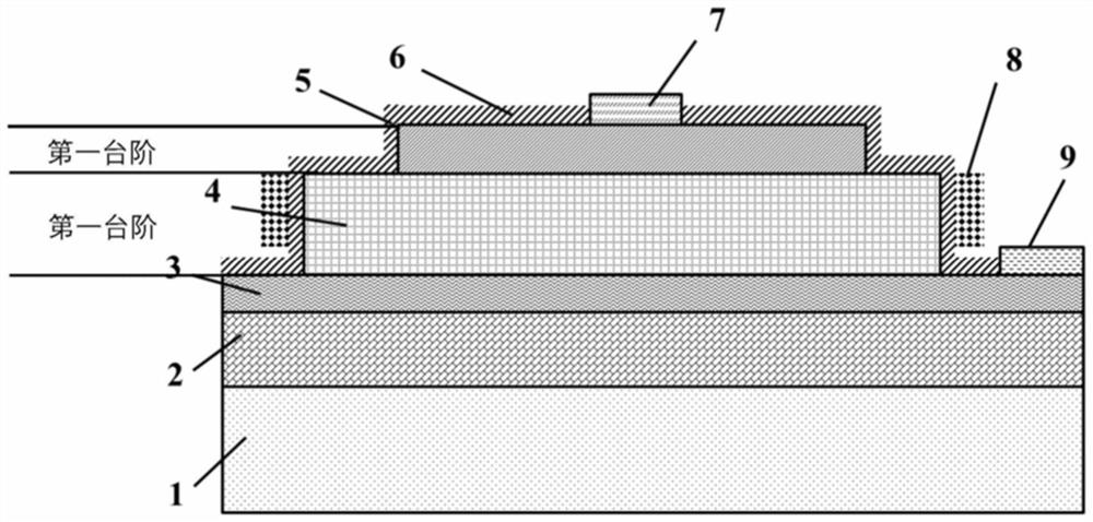
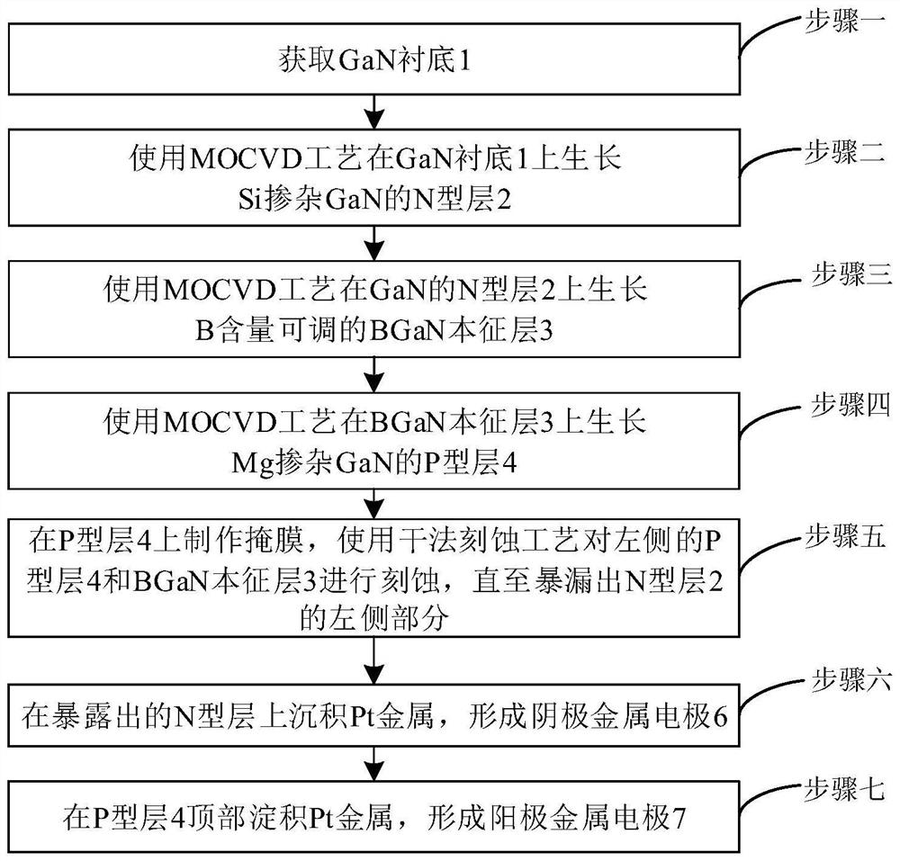
[0026] like figure 2 As shown, a preparation method of a PIN multi-purpose diode with a GaN / BGaN / GaN structure provided by the present invention includes:
[0027] Step 1: Obtain GaN substrate 1;
[0028] Step 2: growing an N-type layer 2 of Si-doped GaN on the GaN substrate 1 using an MOCVD process;
[0029] Among them, the thickness of the N-type layer 2 is 50-300 nm; the process conditions for growing the N-type layer of Si-doped GaN with a thickness of 200 nm are: temperature 1000 ° C, pressure 300 Torr, gallium source flow 100 sccm, Si source flow 50 sccm, ammonia flow 20000 sccm , the hydrogen flow rate is 40000sccm.
[0030] Step 3: growing a BGaN intrinsic layer 3 with adjustable B content on the N-type layer 2 of GaN using MOCVD process;
[0031] Wherein, the content of B is adjusted in the range of 10%-30%, and the thickness of the BGaN intrinsic layer 3 is 30-200 nm. The process conditions for the grown BGaN intrinsic layer 3 are: temperature 1000° C., pressure...
Embodiment 1
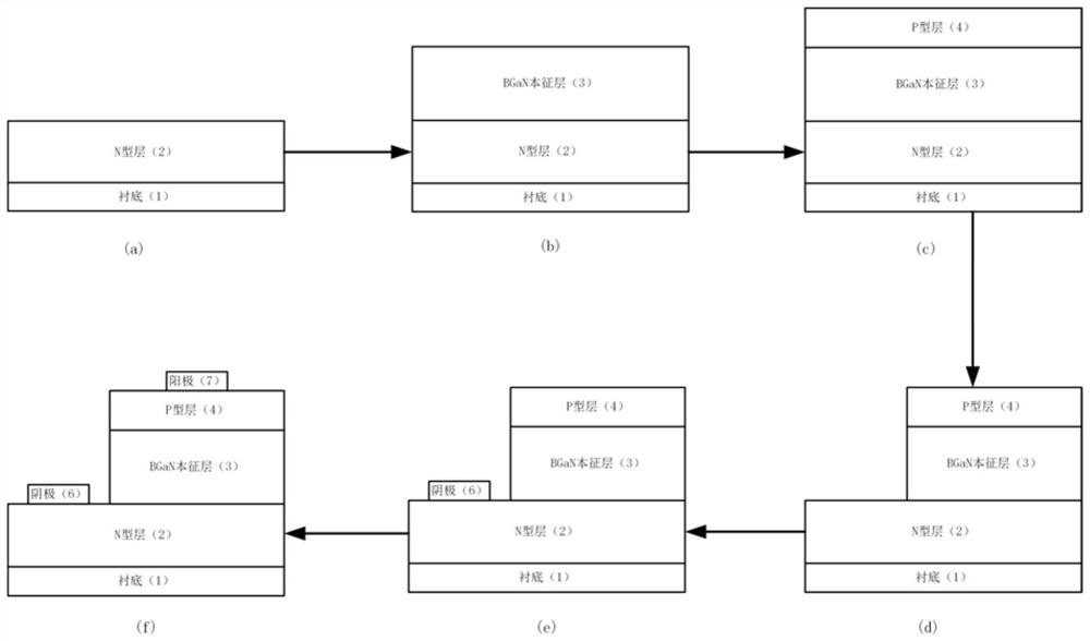
[0041] step 1, as image 3 As shown in the neutron diagram a, 200nm Si-doped GaN was grown on a GaN substrate by MOCVD process. The process conditions are: temperature 1000℃, pressure 300Torr, gallium source flow rate 100sccm, Si source flow rate 50sccm, ammonia gas flow rate 20000sccm, hydrogen gas flow rate Flow 40000sccm;
[0042] step 2, as image 3 As shown in neutron diagram b, a 100nm BGaN intrinsic layer was grown on the GaN N-type layer using MOCVD process, where the B content was 15%, and the process conditions were: temperature 1000°C, pressure 300Torr, gallium source flow 80sccm, B source flow 30sccm, ammonia flow 20000sccm, hydrogen flow 40000sccm
[0043] step 3, as image 3 As shown in neutron diagram c, 200nm Mg-doped GaN was grown on the BGaN intrinsic layer by MOCVD process. The process conditions were: temperature 1000℃, pressure 300Torr, gallium source flow rate 100sccm, Mg source flow rate 500sccm, ammonia gas flow rate 20000sccm, Hydrogen flow 40000sc...
Embodiment 2
[0048] step 1, as image 3 As shown in the neutron diagram a, 200nm Si-doped GaN was grown on a GaN substrate by MOCVD process. The process conditions are: temperature 1000℃, pressure 300Torr, gallium source flow rate 100sccm, Si source flow rate 50sccm, ammonia gas flow rate 20000sccm, hydrogen gas flow rate Flow 40000sccm;
[0049] step 2, as image 3 As shown in the neutron diagram b, a 100nm BGaN intrinsic layer was grown on the GaN N-type layer using the MOCVD process, where the B content was 20%, and the process conditions were: temperature 1000 ° C, pressure 300 Torr, gallium source flow 80sccm, B source flow 40sccm, ammonia flow 20000sccm, hydrogen flow 40000sccm
[0050] step 3, as image 3 As shown in neutron diagram c, 200nm Mg-doped GaN was grown on the BGaN intrinsic layer by MOCVD process. The process conditions were: temperature 1000℃, pressure 300Torr, gallium source flow rate 100sccm, Mg source flow rate 500sccm, ammonia gas flow rate 20000sccm, Hydrogen f...
PUM
| Property | Measurement | Unit |
|---|---|---|
| thickness | aaaaa | aaaaa |
| thickness | aaaaa | aaaaa |
Abstract
Description
Claims
Application Information
 - R&D
- Intellectual Property
- Life Sciences
- Materials
- Tech Scout
- Unparalleled Data Quality
- Higher Quality Content
- 60% Fewer Hallucinations
Browse by: Latest US Patents, China's latest patents, Technical Efficacy Thesaurus, Application Domain, Technology Topic, Popular Technical Reports.
© 2025 PatSnap. All rights reserved.Legal|Privacy policy|Modern Slavery Act Transparency Statement|Sitemap|About US| Contact US: help@patsnap.com