Silicon-based GaN HEMT heat dissipation enhanced packaging structure and preparation method thereof

A packaging structure, silicon-based technology, applied in semiconductor/solid-state device manufacturing, semiconductor/solid-state device components, semiconductor devices, etc., can solve the problem of high difficulty in growing GaN epitaxial wafers on diamond substrates, and cannot solve heat accumulation and heat dissipation Complex structure and other issues to avoid heat accumulation effect, facilitate mass production and improve heat dissipation

Pending Publication Date: 2022-08-05
NANJING UNIV OF POSTS & TELECOMM +1
View PDF2 Cites 0 Cited by
  • Summary
  • Abstract
  • Description
  • Claims
  • Application Information

AI Technical Summary

Problems solved by technology

[0004] The traditional heat dissipation structure of the package often optimizes the heat dissipation capacity of the chip bonding place, the package substrate, the frame, etc., but cannot solve the heat accumulation caused by the silicon substrate of the silicon-based GaN HEMT.
Chinese invention patent CN202111248653.8 discloses a near-junction heat dissipation method for silicon-based gallium nitride devices. It etches the substrate and injects cooling liquid to form heat dissipation channels to enhance the heat dissipation capability of GaN HEMTs, but it needs to inject cooling at all times. Liquid, complex heat dissipation structure; Chinese invention patent CN202111397484.4 discloses a normally-off GaN HEMT structure with enhanced heat dissipation and its preparation method, which utilizes the high thermal conductivity of diamond in GaN devices on diamond substrates to enhance GaN HEMT Excellent heat dissipation performance, but the growth of gallium nitride epitaxial wafers on diamond substrates is difficult and expensive

Method used


Image

  • Silicon-based GaN HEMT heat dissipation enhanced packaging structure and preparation method thereof
  • Silicon-based GaN HEMT heat dissipation enhanced packaging structure and preparation method thereof
  • Silicon-based GaN HEMT heat dissipation enhanced packaging structure and preparation method thereof

Examples


Embodiment 1

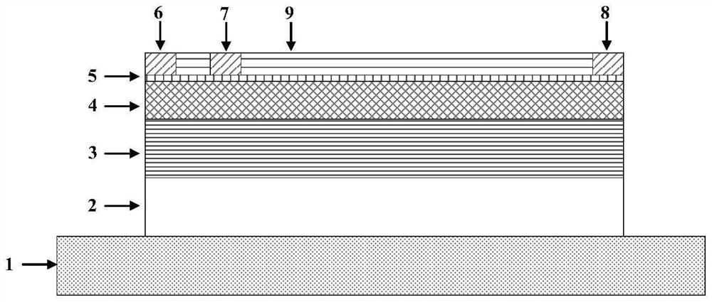
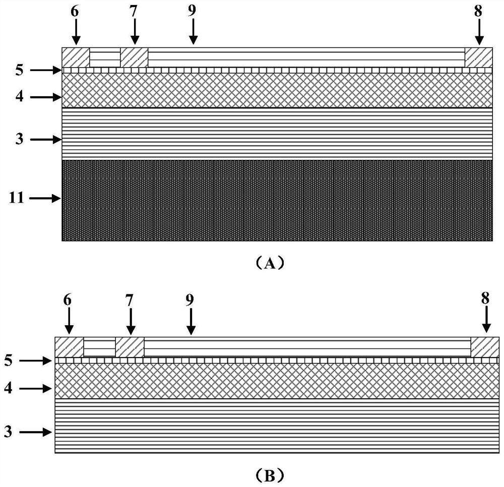
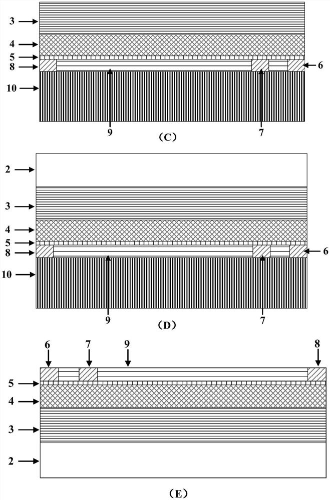
[0034] A silicon-based GaN HEMT (gallium nitride high electron mobility transistor) heat dissipation enhanced packaging structure is prepared by the following steps:

[0035] Step 1), cleaning the silicon substrate;

[0036] Step 2), on the silicon substrate, using metal organic chemical vapor deposition to sequentially epitaxially grow the GaN buffer layer, the GaN channel layer and the AlGaN barrier layer to obtain a silicon-based gallium nitride epitaxial wafer;

[0037] Step 3), using PECVD to coat the surface of the epitaxial wafer in step 2) with silicon nitride dielectric material, passivating the surface of the AlGaN barrier layer, reducing the interface state density, and obtaining a passivation epitaxial wafer;

[0038] Step 4), using chemical mechanical polishing to flatten the surface of the epitaxial wafer passivated in step 3);

[0039] Step 5), performing patterned etching of the source ohmic electrode and the drain ohmic electrode;

[0040] Step 6), vapor dep...


PUM

PropertyMeasurementUnit
thicknessaaaaaaaaaa
thicknessaaaaaaaaaa
thicknessaaaaaaaaaa

Abstract

The invention discloses a silicon-based GaN HEMT (High Electron Mobility Transistor) heat dissipation enhanced packaging structure and a preparation method thereof, and belongs to the field of information materials and devices, the structure takes a substrate (1) as a carrier and is connected with a high heat conduction layer (2) in a chip bonding mode, the upper part of the high heat conduction layer (2) is connected with a GaN HEMT, and the lower part of the high heat conduction layer (2) is connected with a silicon-based GaN HEMT. The GaN HEMT sequentially comprises a GaN buffer layer (3), a GaN channel layer (4), an AlGaN barrier layer (5), a medium passivation layer (9) and a metal electrode from bottom to top. According to the prepared structure, the low-heat-conductivity silicon substrate of the silicon-based GaN HEMT is peeled off, the high-heat-conductivity material is connected with the substrate, the heat accumulation effect caused by the silicon-based material is avoided, the heat dissipation capacity of the high-power-density GaN HEMT chip is improved, the structure is compatible with an existing advanced packaging structure and a packaging heat dissipation technology, and the manufacturing cost is reduced. The electric heating performance and the reliability of the packaged chip can be remarkably improved, and the high value is achieved.

Description

technical field [0001] The invention belongs to the field of information materials and power device packaging, and in particular relates to a silicon-based GaN HEMT heat dissipation enhanced packaging structure and a preparation method thereof. Background technique [0002] As a typical third-generation semiconductor power device, GaN HEMT benefits from the unique characteristics of GaN material, such as wide band gap, high electron saturation drift rate and high critical breakdown electric field, as well as high concentration and high mobility at the AlGaN / GaN heterojunction. It has the advantages of high power density, high breakdown voltage, and low on-resistance, so it is widely used in aerospace, 5G base stations, power electronics and new energy vehicles. ,with broadly application foreground. [0003] Since silicon-based GaN has a higher cost advantage than silicon carbide epitaxial GaN substrates and GaN free-standing substrates, it can achieve lower defect density a...

Claims


Application Information

Patent Timeline
Patent Type & Authority Applications(China)
IPC IPC(8): H01L23/373H01L29/778H01L21/78H01L21/50H01L21/335
CPCH01L23/3736H01L23/3738H01L23/3732H01L29/7787H01L29/66462H01L21/7813H01L21/50
Inventor 刘建华郭宇锋姚清姚佳飞张茂林杨航蔡志匡
Owner NANJING UNIV OF POSTS & TELECOMM
Why Eureka
Try Eureka