Polishing method
A substrate and power technology, applied in the polishing field, can solve the problems of prolonged processing time, increased manufacturing cost, and inability to obtain ionization energy.
- Summary
- Abstract
- Description
- Claims
- Application Information
AI Technical Summary
Problems solved by technology
Method used
Image

Examples
Embodiment Construction
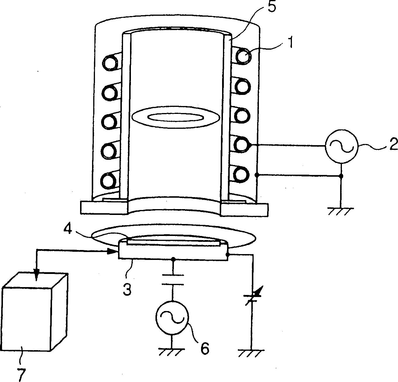
[0019] The polishing method of the present invention is a method performed to remove a resist mask formed through an insulating film at least on a substrate.
[0020] As substrates usable in the present invention are generally all substrates used for manufacturing semiconductor devices, such as glass substrates, plastic substrates, semiconductor substrates, semiconductor wafers, and the like. Specifically, various substrates such as elemental semiconductor (silicon, germanium, etc.) substrates, compound semiconductors (GaAs, ZnSe, silicon germanium, etc.) substrates, substrates such as SOI, SOS, etc. Quartz substrate, plastic (polyethylene, polystyrene, polyimide, etc.), etc. Elements such as transistors, capacitors, and resistors, circuits including these elements, interlayer insulating films, wiring layers, and the like can be formed on the substrate.
[0021] As the insulating film formed on the substrate, for example, it is usually formed as an interlayer insulating film,...
PUM
 Abstract
Description
Claims
Application Information