Electrooptic device, manufacturing method thereof, liquid crystal device and projective display device

A technology of electro-optic devices and manufacturing methods, applied in semiconductor/solid-state device manufacturing, electric solid-state devices, electrical components, etc., can solve problems such as smaller aperture ratio, difficulty in improving pixel integration, charge leakage, etc., to prevent excessive current carrying The effect of suppressing the accumulation of sub-substrates, suppressing the floating effect of the substrate, and preventing the flow of leakage current

Inactive Publication Date: 2005-12-07
BOE TECH GRP CO LTD
View PDF1 Cites 0 Cited by
  • Summary
  • Abstract
  • Description
  • Claims
  • Application Information

AI Technical Summary

Problems solved by technology

[0011] However, when body contact regions are provided for MIS transistors used in the pixel regions of electro-optical devices represented by liquid crystal devices, it is difficult to increase the integration of pixels due to the increase in the area occupied by each MIS transistor, especially in transmissive In the case of liquid crystal devices, there is a problem that the aperture ratio becomes smaller
In addition, providing a body contact region in the peripheral driver circuit other than the pixel region also makes integration difficult, and there is a problem that the peripheral portion (frame portion) of the device is enlarged, and miniaturization cannot be achieved.
[0012] In addition, in electro-optical devices used in electronic devices such as projection display devices, when strong light from a light source enters the channel region and LDD region (lightly doped drain) of a pixel transistor, a current will be generated due to light excitation. The charge leaks from the pixel storage capacitor, and the result is the cause of display unevenness such as flickering

Method used


Image

  • Electrooptic device, manufacturing method thereof, liquid crystal device and projective display device
  • Electrooptic device, manufacturing method thereof, liquid crystal device and projective display device
  • Electrooptic device, manufacturing method thereof, liquid crystal device and projective display device

Examples


Embodiment Construction

[0064] Refer below Figure 1 to Figure 8 An embodiment of the present invention will be described.

[0065] In this embodiment, as an example of the electro-optical device of the present invention, an example of a liquid crystal light valve (liquid crystal device) used as a light modulation device of a projection display device will be described. The liquid crystal light valve of this embodiment is an active matrix mode liquid crystal panel, and an SOQ substrate is used on the element substrate side.

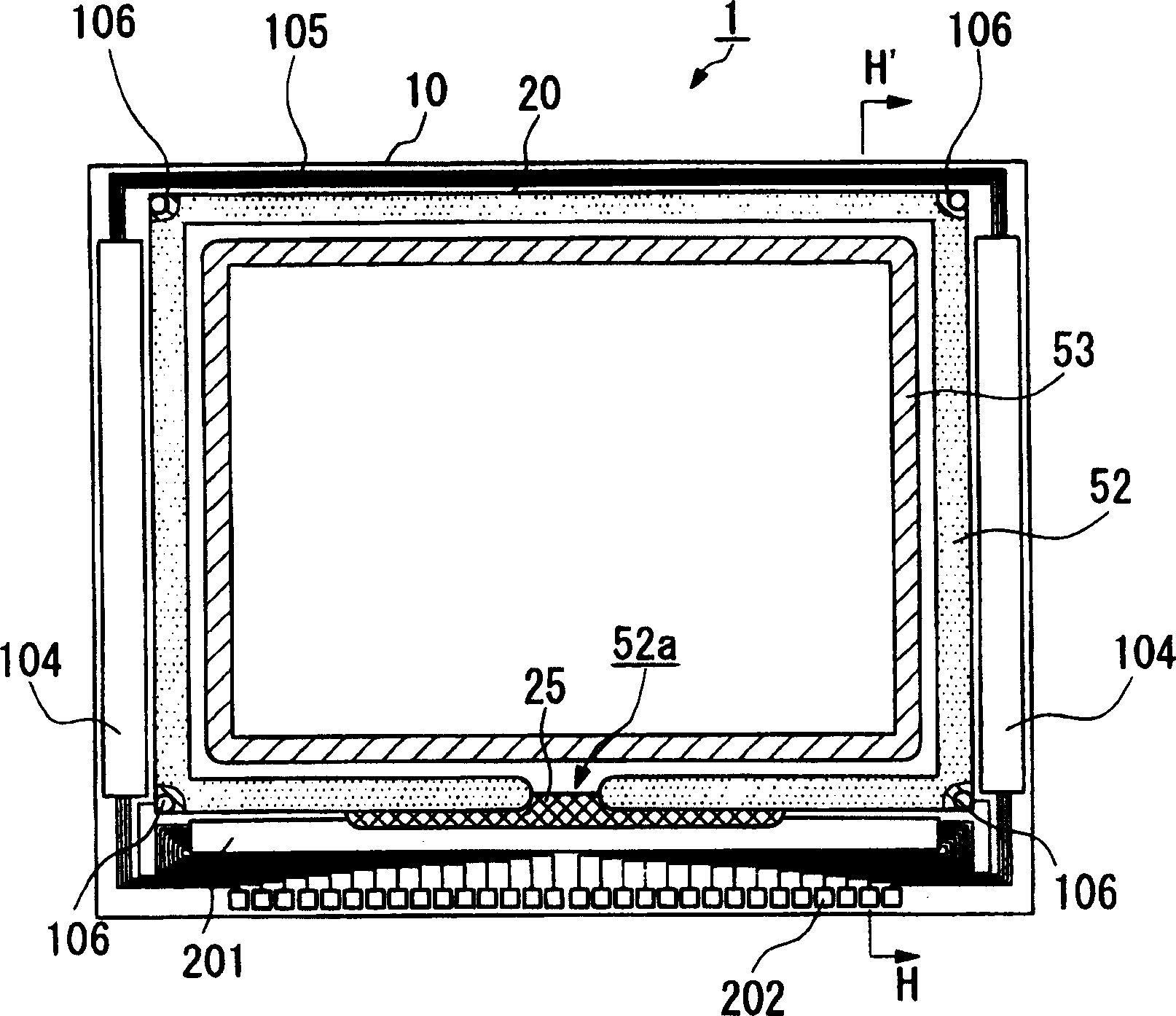
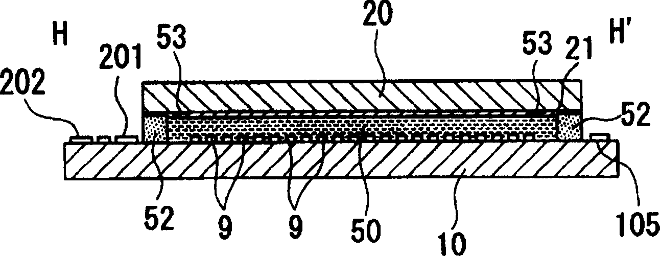
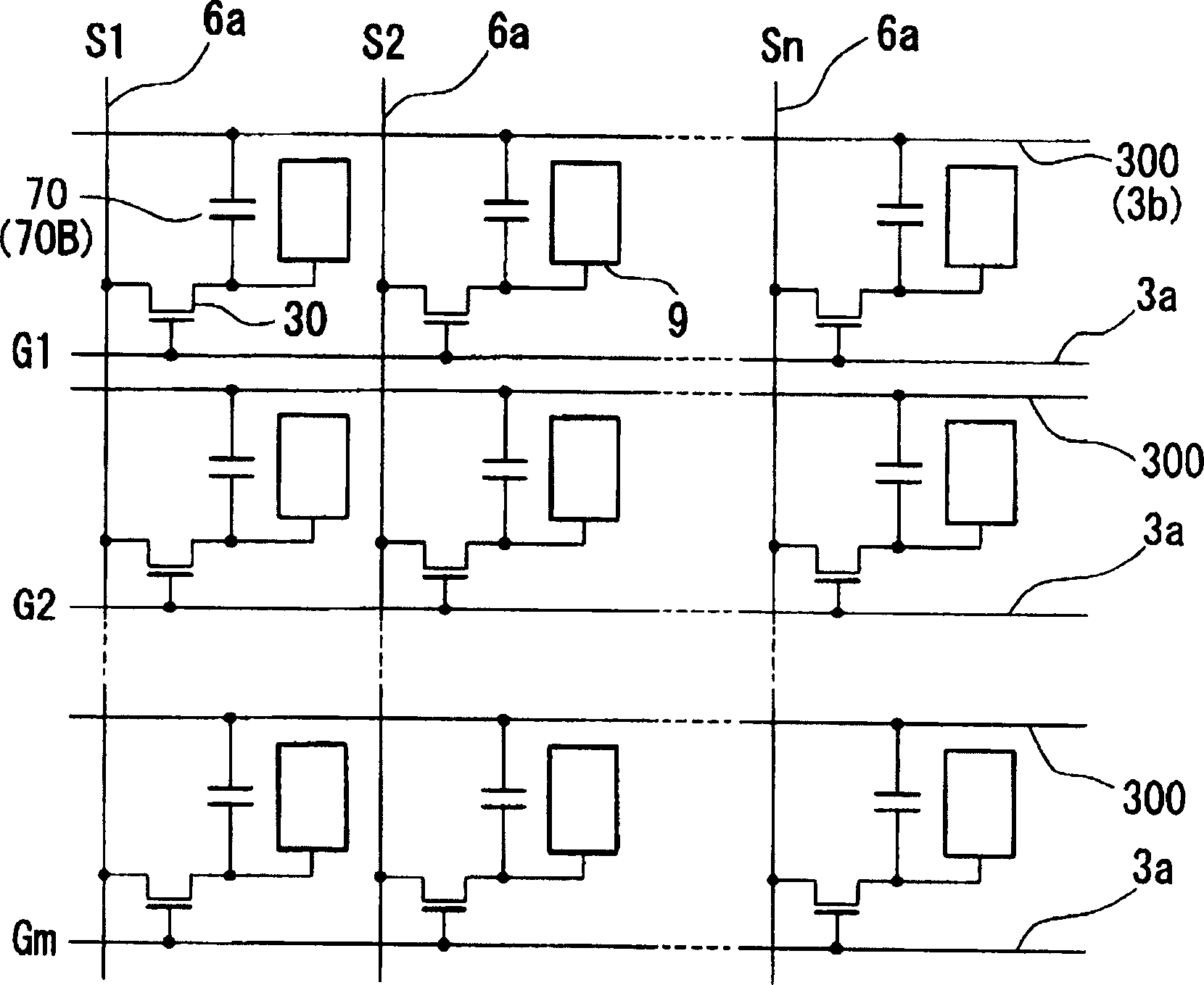
[0066] figure 1 is a schematic configuration diagram of a liquid crystal light valve as an example of the electro-optic device of the present invention, figure 2 is along figure 1 The profile of the H-H' line, image 3 It is an equivalent circuit diagram of a plurality of pixels forming a matrix to form a liquid crystal light valve, Figure 4 is the planar view of multiple pixel groups, Figure 5 is along Figure 4 The profile of the line A-A', Figure 6 It is a cross-s...


PUM

PropertyMeasurementUnit
thicknessaaaaaaaaaa

Abstract

To provide an electrooptic device which can reliably suppress a substrate floating effect, such as a parasitic bipolar phenomenon, in an SOI-MIS transistor, and which has superior electrical characteristics. An electrooptic device (liquid crystal light valve) of the present invention uses, as one substrate, a composite substrate including a quartz substrate (main substrate 10A) having a first coefficient of thermal expansion, an insulating layer (insulating underlayer 12) formed on the quartz substrate, and a single-crystal silicon layer (semiconductor layer 1a) formed on the insulating layer and having a second coefficient of thermal expansion. A TFT 30 that uses the single-crystal silicon layer as a channel region 1a' is formed on the insulating layer, and at least one line defect D exists in the single-crystal silicon layer that forms the channel region 1a'.

Description

technical field [0001] The present invention relates to an electro-optical device, a liquid crystal device, and a projection display device, and particularly relates to a structure of an electro-optic device such as a liquid crystal device suitable for use in a projection display device, which can sufficiently suppress the floating effect of a substrate. Background technique [0002] The SOI (silicon on insulator) technology, in which a semiconductor layer composed of a single crystal silicon layer is formed on an insulator layer, and semiconductor devices such as transistor elements are formed on the semiconductor layer, has the advantages of high speed, low power consumption, and high integration. , for example, can be applied to electro-optical devices such as liquid crystal devices. [0003] However, in general bulk semiconductor devices, since the channel region of the MIS (Metal-Insulator-Silicon) transistor can be fixed at a predetermined potential through the base su...

Claims


Application Information

Patent Timeline
Patent Type & Authority Patents(China)
IPC IPC(8): G02F1/13G02F1/1333G02F1/136G02F1/1362G02F1/1368H01L21/02H01L21/336H01L27/12H01L29/786
CPCG02F1/1368G02F2201/40G02F2001/136263G02F1/136277G02F1/136263G02F1/136
Inventor 片山茂宪
Owner BOE TECH GRP CO LTD
Why Eureka
Try Eureka