

Incoherent light-emitting device for driving vertical laser cavity
A technology of organic light-emitting devices and laser cavities, which is applied to laser components, lasers, phonon exciters, etc., can solve problems such as difficult to determine devices, and achieve the effects of low scattering/absorption loss and high light output
- Summary
- Abstract
- Description
- Claims
- Application Information
AI Technical Summary
Problems solved by technology
Method used
Image

Examples
example 1
[0056] To determine the general lasing characteristics of the organic solid-state laser device depicted in Figure 2, a vertical laser cavity structure was formed on a pre-cleaned 4-inch silicon substrate. On the surface of the substrate, the DBR mirror is deposited by the traditional electron beam deposition method, which consists of Ta 2 o 5 and SiO 2 of alternating high and low refractive index layers. The formed mirror layer has a reflection blocking band greater than 99% between 600nm and 720nm, and its reflectivity is greater than 99.999% at the central wavelength of 660nm. On the top surface of the lower DBR mirror, an active layer consisting of 200nm Alq doped with 1% DCJTB was deposited by high vacuum thermal evaporation. Finally, the upper DBR mirror was deposited using a low temperature electron beam deposition technique, during which the measured temperature of the silicon substrate was kept below 72 °C. It consists of alternating high and low refractive index l...
example 2
[0061] In this example, a vertical laser cavity structure similar to that described in Example 1 will be discussed. Three cavities (using a silicon substrate) nominally designed to lase at 660 nm were fabricated. The active layer thickness of cavity A is λ 1 / 2n(=195nm); the active layer thickness of cavity B is λ 1 / n(=390nm); the active layer thickness of cavity C is 2λ 1 / n (=780nm). All three active layers consist of Alq, doped with 1% DCJTB. The upper and lower DBR mirrors are the same in all three cases and are made as described below. The lower DBR mirror consists of alternating high and low refractive index layers of titanium dioxide and silicon dioxide, respectively. The formed mirror has a reflection stop band greater than 99% between 580nm and 750nm, and its reflectivity is greater than 99.999% at the central wavelength of 665nm. In addition, the mirror has a broad reflection maximum at 445nm with a peak reflectivity greater than 92%. The upper DBR mirror als...
example 3
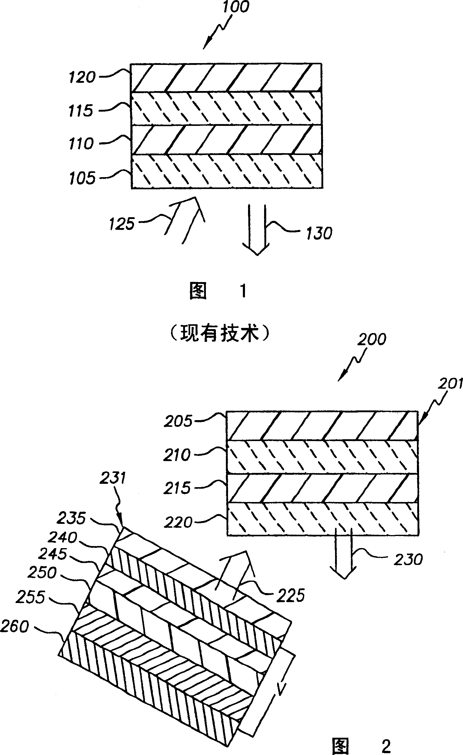
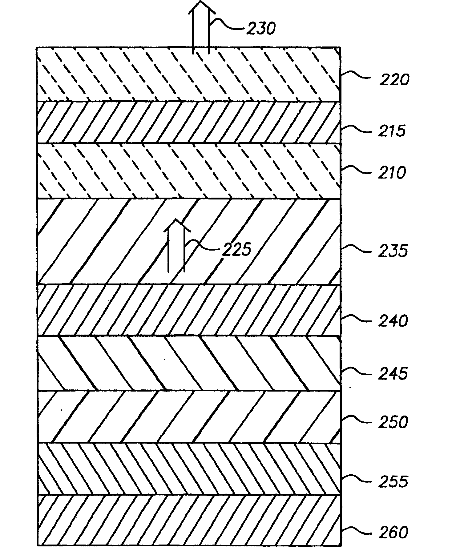
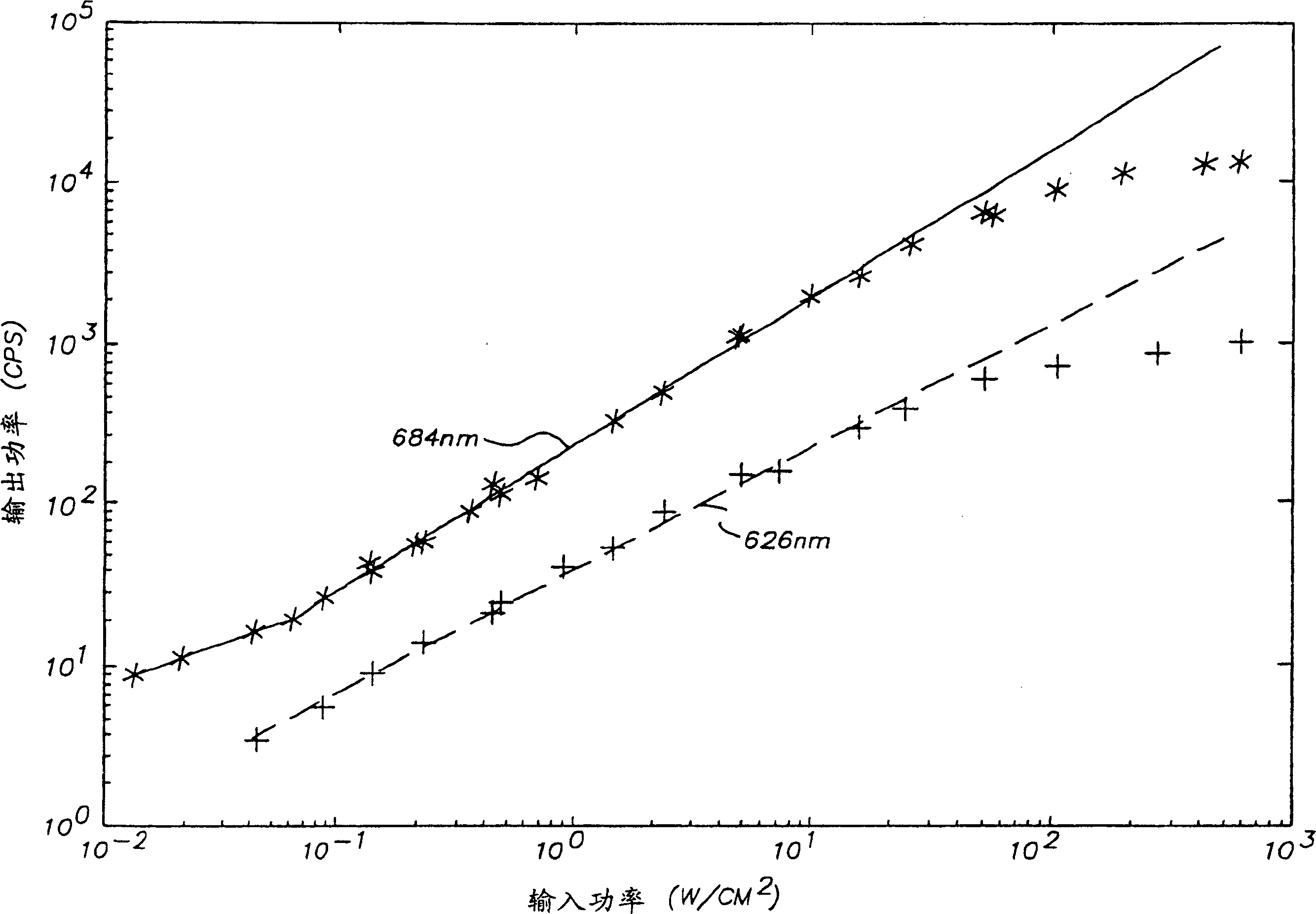
[0067] This is an example of an embodiment given in FIG. 2 where the incoherent light output 225 from the OLED 231 is used to drive the vertical laser cavity structure 201 . Cavities A and B, as described in Example 2, were used as vertical laser cavity structures, while OLED devices were fabricated as follows:
[0068] a) 85 nm thick transparent anodes of ITO-coated glass were subjected to ultrasonic treatment in a commercial detergent, washed in deionized water, degreased in toluene vapor, and then exposed to a strong oxidizing agent;
[0069]b) A 150nm thick NPB hole transport layer is deposited on the ITO anode by conventional thermal vapor deposition;
[0070] c) A 30nm thick ADN light-emitting layer is deposited on the NPB layer by conventional thermal vapor deposition;
[0071] d) A 20nm thick Alq electron transport layer is deposited on the light-emitting layer by conventional thermal vapor deposition;
[0072] e) A 100 nm thick MgAg cathode is deposited on the elect...
PUM
 Abstract
Description
Claims
Application Information