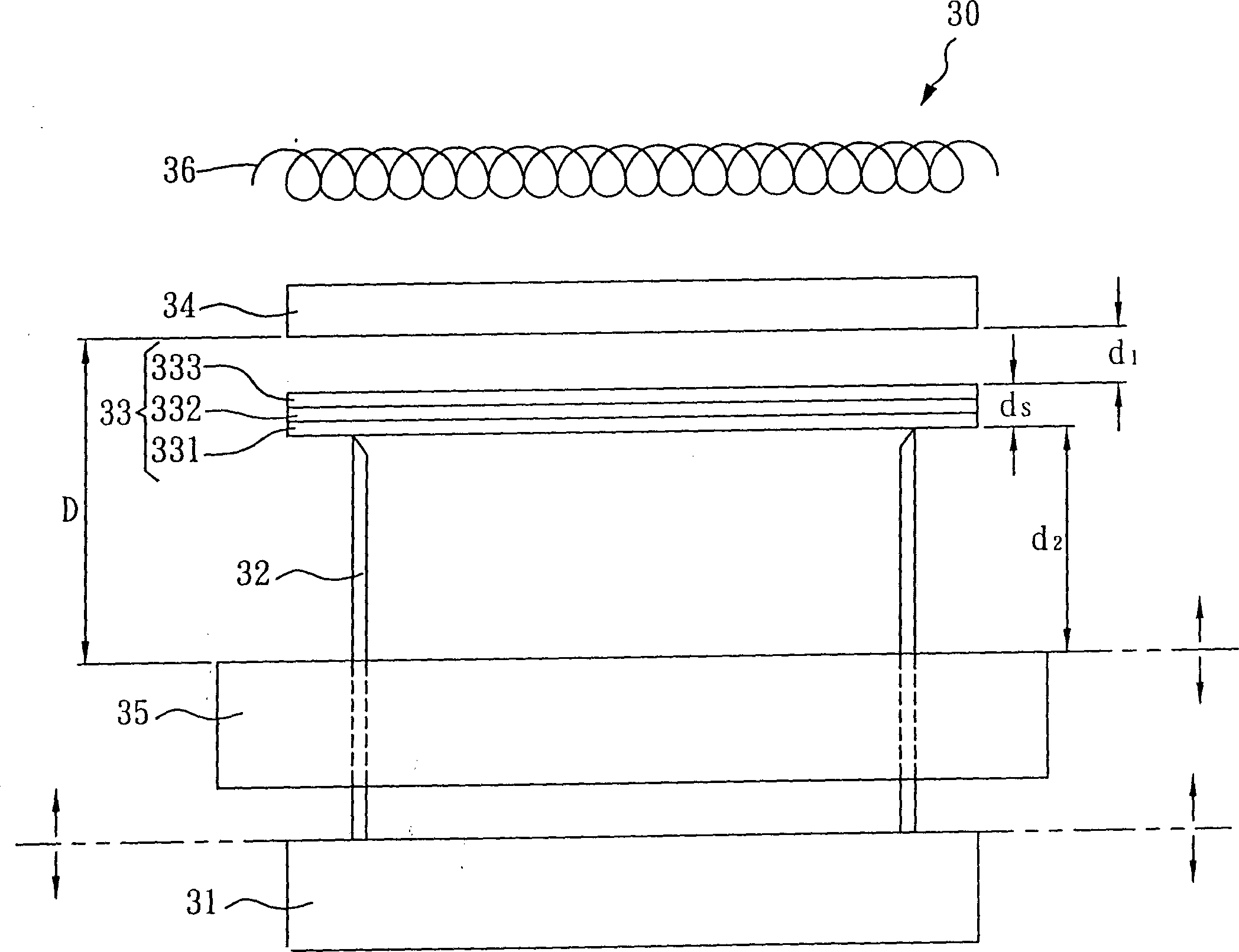
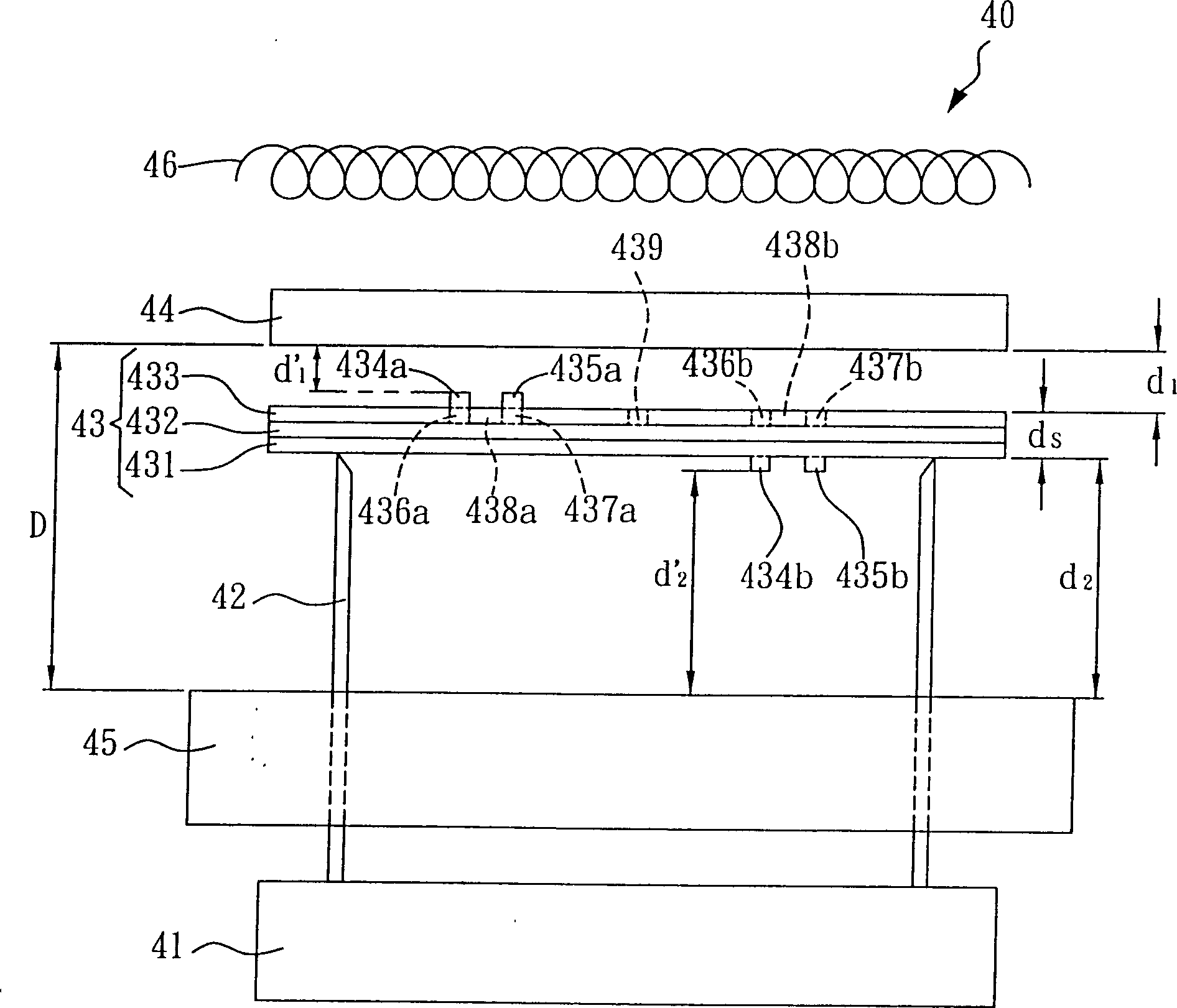
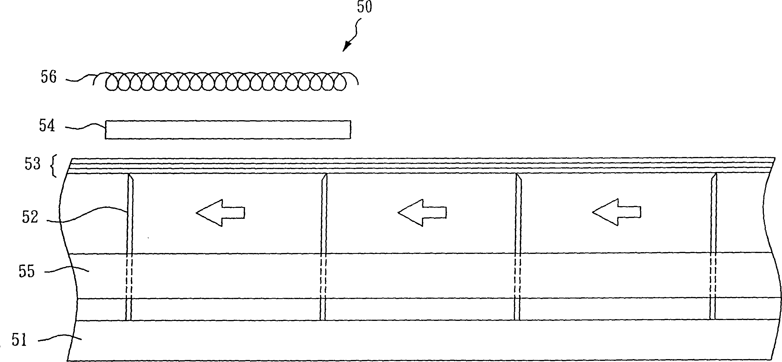
[0005] 1.
Excimer laser annealing equipment is very expensive
[0007] 3. Scanning annealing treatment of large-area substrates is time-consuming and labor-intensive
[0008] 4. Due to the growth and pushing effect between the
crystallization regions (grains), some regions are raised and some regions are sunken, resulting in the absence of
high surface roughness and poor uniformity of the polysilicon film layer
[0010] 1. Due to the low temperature (400°C-600°C), the growth rate of each
crystallization region of the polysilicon thin film layer produced by the furnace annealing method is slow, and the production capacity is limited
[0011] 2. Due to the low temperature (400°C-600°C), the energy provided is low, and the crystallization regions of the polysilicon thin film layer made by the furnace tube annealing method are small, and the
conductivity is lower than that of the polysilicon thin film layer made by
laser annealing[0022] In the above first and second research papers on pulsed
rapid thermal annealing, according to the experimental description, an
amorphous silicon film is deposited on a
single crystal silicon (
crystalline silicon, referred to as C-Si) substrate,
single crystal silicon substrate A
silicon dioxide layer is added between the
amorphous silicon thin film layer, and a
nickel metal layer is plated on the amorphous
silicon thin film layer to induce crystallization, and a
tungsten halogen lamp (
tungsten halogen lamp) is used to test directly on the top The film is pulsed to irradiate; the two research papers adopt the commonly used annealing method, that is, the method of directly irradiating the test piece with
infrared photons emitted by the tungsten-
halogen lamp, but in fact the amorphous
silicon thin film layer is harmful to the The absorption coefficient of
infrared photons of
tungsten filament lamps is very small and cannot be effectively absorbed. The energy for converting amorphous
silicon thin film layers into polysilicon thin films mainly comes from the
heat energy released by the
single crystal silicon substrate absorbing
infrared photons of
tungsten filament halogen lamps. The
crystalline silicon thin film layer is effectively annealed into polysilicon by being irradiated by the lamp; in addition, the
single crystal silicon substrate also fails to meet the aforementioned requirements of integrating low-temperature polysilicon into a glass or a plastic substrate
[0023] In the above 3rd to 6th research papers on pulse
rapid thermal annealing, according to the experimental description, the amorphous silicon thin film layer is deposited on a glass substrate (the third paper is between the amorphous silicon thin film layer and the glass substrate. A
silicon nitride layer is added in between, and a
thin metal layer is plated on top of the amorphous silicon film layer to induce crystallization), a
single crystal silicon stage is used to carry the glass substrate and measure the temperature, and a tungsten-filament
halogen lamp is used to automatically The pulsed
irradiation is directly applied to the amorphous silicon thin film layer, glass substrate and
single crystal silicon stage; the four research papers still use the commonly used annealing method, that is, the infrared photons emitted by the tungsten
halogen lamp are directly irradiated. In fact, the absorption coefficient of the amorphous silicon thin film layer to the infrared photons of the halogen lamp is very small and cannot be effectively absorbed, so that the energy of the
polycrystalline silicon thin film converted from the amorphous silicon thin film layer mainly comes from the absorption of infrared photons from the
tungsten filament halogen lamp. The energy released by the polysilicon stage is not that the amorphous silicon film layer is effectively annealed into polysilicon by the lamp; in addition, the
heat energy released by the single
crystal silicon stage must first be conducted through the glass substrate before reaching the amorphous silicon film Therefore, the conventional technology of pulse
rapid thermal annealing disclosed in four research papers, when using high-temperature pulses, heat energy will first be transmitted to the glass and then to the amorphous silicon film layer, so it is extremely easy to damage the glass substrate
[0024] The pulse rapid thermal annealing method adopted in the above prior art all adopts the commonly used annealing method, that is, the method in which the infrared photons emitted by the tungsten halogen lamp directly irradiate the test piece. The
photon absorption coefficient is small and the
absorption effect is poor. The amorphous silicon thin film layer cannot be heated by infrared
photon irradiation. In fact, the single
crystal silicon substrate or single
crystal silicon carrier absorbs the energy of infrared photons emitted by the tungsten halogen lamp.
When the single crystal silicon is not used as the substrate or the stage, the amorphous silicon thin film layer cannot effectively use the method of infrared photons to directly irradiate the test piece to achieve the effect of annealing into a single crystal silicon thin film
In addition,
monocrystalline silicon cannot meet the above-mentioned requirement of integrating low-temperature polysilicon into a glass or a plastic substrate.


