Ultrathin pinless packaging process of integrated circuit and discrete component and its packaging structure

A discrete component, integrated circuit technology, applied in the field of integrated circuit or discrete component ultra-thin leadless packaging process and its packaging structure, can solve the problems of rigid arrangement, high electroplating cost, discount on utilizability, etc., achieve high transmission and heat dissipation, The effect of low material cost and stable quality

Active Publication Date: 2007-01-17
长电科技管理有限公司
View PDF6 Cites 1 Cited by
  • Summary
  • Abstract
  • Description
  • Claims
  • Application Information

AI Technical Summary

Problems solved by technology

[0004] 2. In order to make the wire bonding process and output solder joints can be produced smoothly in this process, expensive palladium materials are plated on both sides of the substrate. In addition to the relatively high cost of electroplating, the wire bonding parameters should also be set for this material Special parameters, which directly affect the smoothness of the production line due to the inconsistency of the parameters
[0005] 3. The substrate is generally made of CU194, which has a conductivity of only 65% ​​and a relatively slow heat dissipation rate. It is only suitable for general logic or low-power products.
[0006] 4. Because of the use of special chemical tape and the solvent of the tape in various high-temperature processes is easy to vaporize due to high temperature, the aluminum pad that indirectly pollutes or covers the chip, that is, the inner foot of the wire, often causes the instability of the wire bonding ability
[0007] 5. Because this product is made of plastic and copper, the same blade and blade rotation speed cannot be used to divide the array integrated circuit or discrete component assembly under different materials, and the two blades cannot be the same, and if When forcing the use of the same blade, that is, the speed parameter, the life of the blade will be greatly reduced. Of course, the maintenance cost and quality will be affected to a certain extent.
[0008] 6. Due to the limitation of traditional technology, solder joints with multiple chips and different outputs can only be arranged in a rigid manner, and the flexibility is greatly reduced.
[0009] 7. Due to the limitation of the traditional process, the output solder joints are as flat as the bottom of the plastic package, and there is even a risk of depression, while flux, rust remover and other chemicals are used for surface mounting. It cannot be discharged smoothly, so it will be greatly reduced in terms of solderability

Method used


Image

  • Ultrathin pinless packaging process of integrated circuit and discrete component and its packaging structure
  • Ultrathin pinless packaging process of integrated circuit and discrete component and its packaging structure
  • Ultrathin pinless packaging process of integrated circuit and discrete component and its packaging structure

Examples


Embodiment Construction

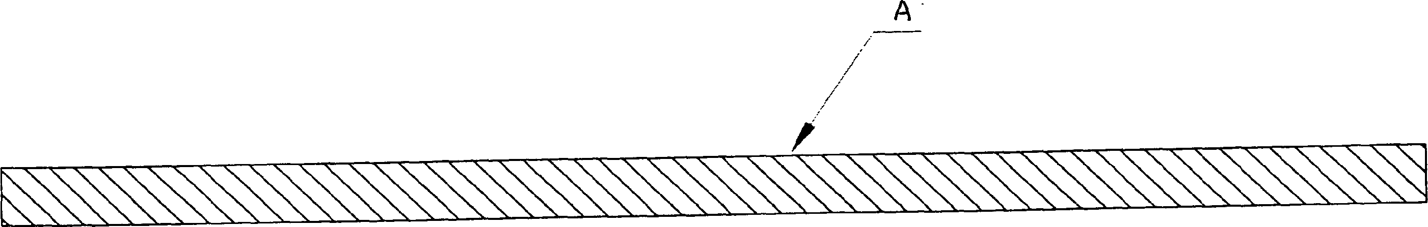
[0046] 1) see figure 1 , take a piece of metal substrate A of suitable thickness. The material of the metal substrate can be changed according to the function and characteristics of the chip, such as: alloy or copper;

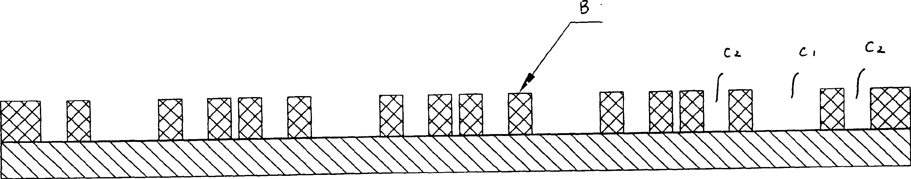
[0047] 2) see figure 2 , Dry ink B coating is carried out on the metal substrate A. The area on the metal substrate that is not coated with dry ink forms the chip area C1 and the inner foot area C2 for wiring;

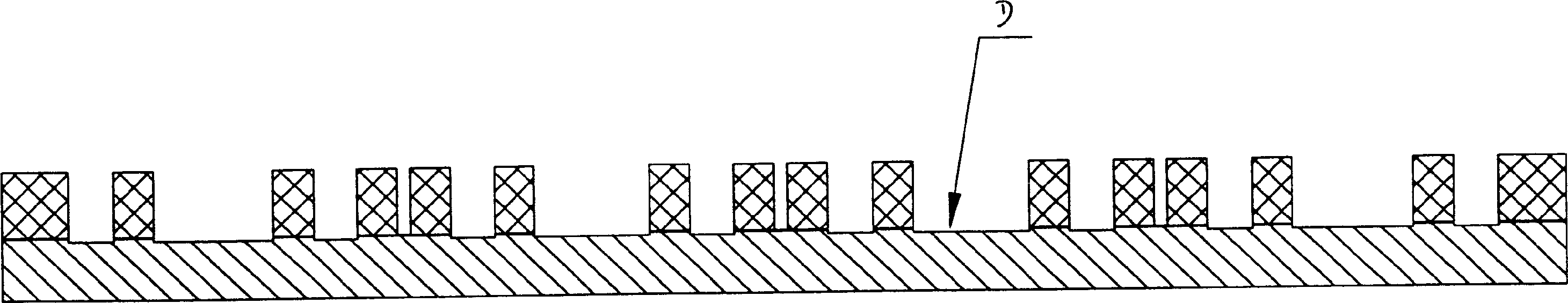
[0048] 3) see image 3 , etching the chip area C1 and the inner foot area C2 of the wire bonding on the metal substrate D;

[0049] 4) see Figure 4 , sputtering a layer of pure metal layer 1 on the metal substrates A1 and A2 in the chip area C1 and the wire-bonding inner foot area C2;

[0050] 5) see Figure 5 , on the pure metals 11 and 12 in the chip area C1 and the wire-bonding inner pin area C2, a layer of metal activation layer 2 is sputtered, such as an aluminum layer or a nickel, titanium, silver, or gold layer;

[0051] 6) see Figure ...


PUM


Abstract

The invention discloses an ultrathin encapsulation technology of integrate circuit or discrete component and includes the following steps: get basal plate, coat dry ink on the basal plate, etch the chip area and inner area of the throwing on the basal plate, coat a film of metals, metallic active layer, copper or alloy layer on the basal plate, plate a coat of argentine or nickel or palladium over the copper or alloy layer in the throwing area, divest the dry ink layer, coat argentine sol on the copper or alloy layer in the chip area, imbed the chip in the argentine sol, throw, encapsulate, print it with laser printer, divest the metallic basal plate, stick it on the blue cutan and comminute the encapsulating bodies. The invention is featured by strong welding, good quality, low cost, smooth production, strong applicability, highest efficiency of the cutting machines and blades, flexible arrangement of the chips and environmental protection and the trouble of the infiltration of plastics won't happen.

Description

Technical field: [0001] The invention relates to an ultra-thin and footless packaging process for integrated circuits or discrete components and a packaging structure thereof. It belongs to the technical field of packaging of integrated circuits or discrete components. Background technique: [0002] The traditional ultra-thin and footless packaging process of integrated circuits or discrete components and its packaging structure, its packaging type is an array-type assembly that is cut into a single unit. Its substrate type is etched. It mainly has the following deficiencies: [0003] 1. Special adhesive tape is required. In order to prevent the plastic from penetrating into the lead frame during high-pressure encapsulation, increasing the risk of solder joint insulation, and if the post-treatment of plastic penetration occurs, it is easy to destroy the metal layer of the solder joint. Affects weldability, so material cost, post-processing cost and quality all have a cert...

Claims


Application Information

Patent Timeline
Patent Type & Authority Patents(China)
IPC IPC(8): H01L21/50H01L21/56H01L21/60H01L21/48
CPCH01L2224/32245H01L24/97H01L2224/48091H01L2224/73265H01L2224/48247H01L2224/48465H01L2224/97H01L2924/14H01L2924/00014H01L2924/00
Inventor 梁志忠黄能捷韩蔚华
Owner 长电科技管理有限公司
Why Eureka
Try Eureka