Method for making electronic component using wet corrosion agent

A manufacturing method and technology for electronic components, which are applied in the fields of semiconductor/solid-state device manufacturing, electrical components, and photoengraving processes of patterned surfaces, can solve the problems of thin thickness, poor operability, and low rigidity, and achieve high etching accuracy and cost. Falling, cheap effects

Inactive Publication Date: 2002-12-18
DAI NIPPON PRINTING CO LTD
View PDF16 Cites 4 Cited by
  • Summary
  • Abstract
  • Description
  • Claims
  • Application Information

AI Technical Summary

Problems solved by technology

[0021] Laminates using polyimide as an insulating layer are thin and have low rigidity, so compared with conventional rigid glass epoxy substrates, etc., there is a problem of so-called poor handleability, so it becomes a big problem in design and processing. constraints

Method used


Image

  • Method for making electronic component using wet corrosion agent
  • Method for making electronic component using wet corrosion agent
  • Method for making electronic component using wet corrosion agent

Examples


Embodiment A

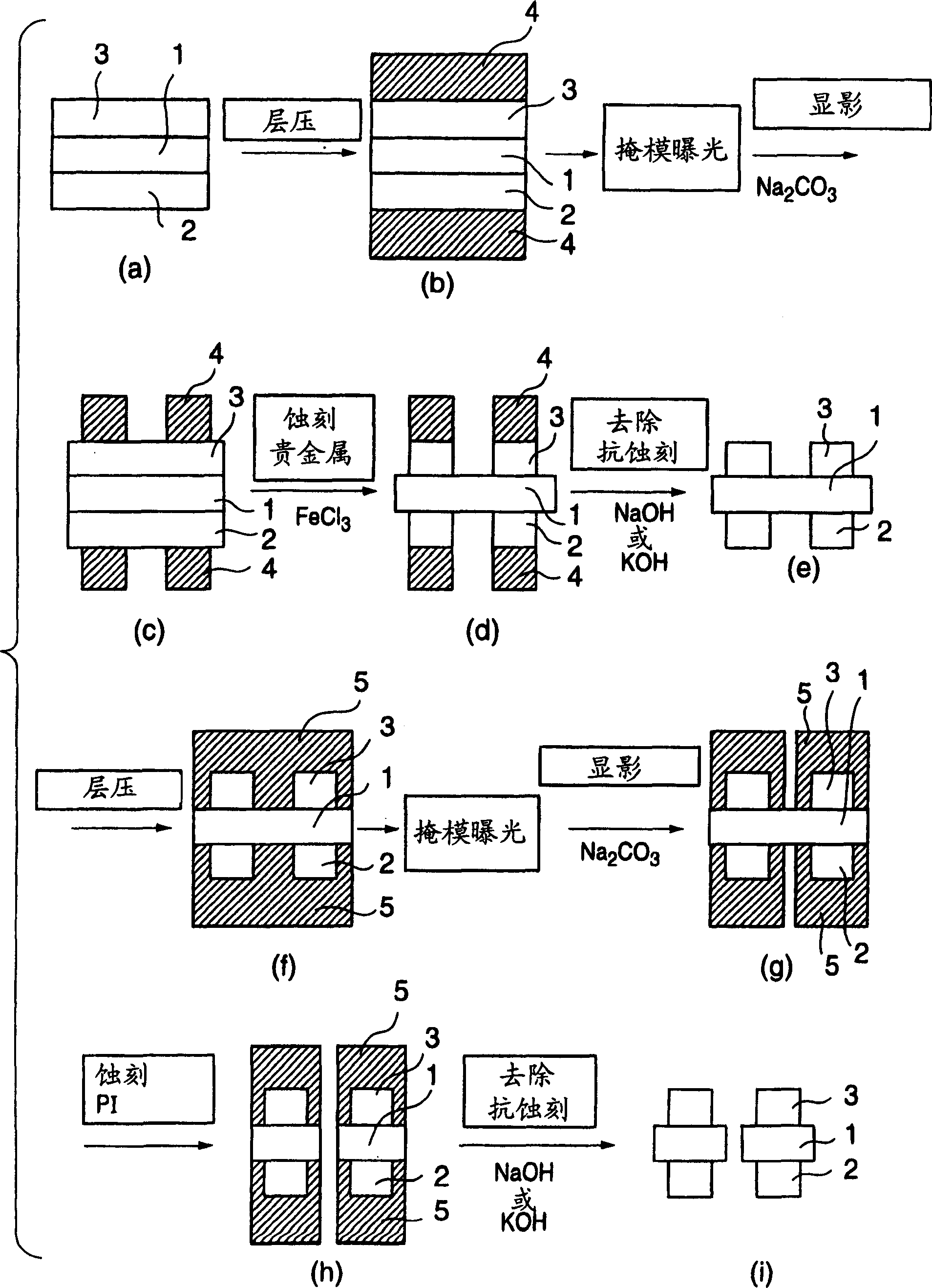
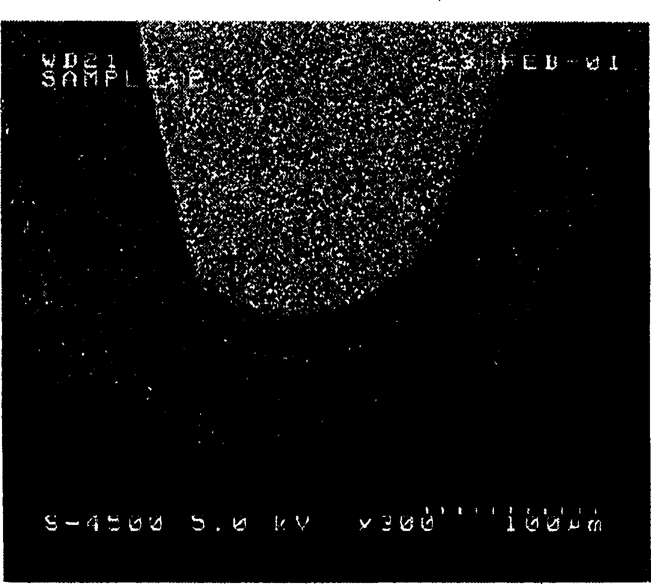
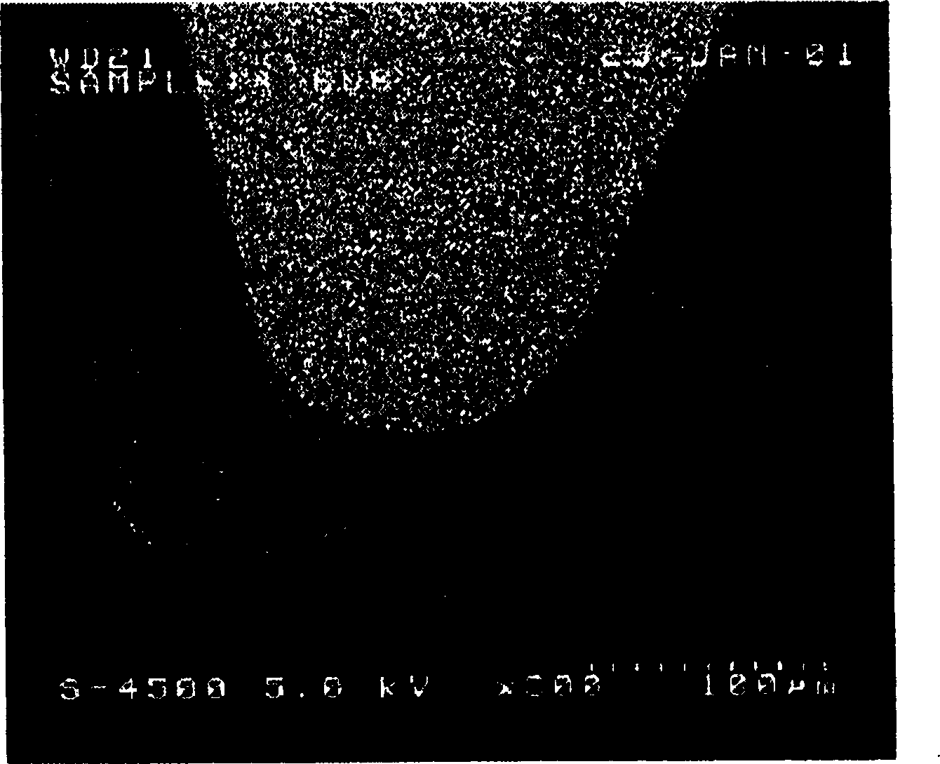
[0248] wet etchable laminate

[0249] [etching test]

[0250] In order to manufacture a sample for forming an insulating layer, a polyamic acid varnish manufactured by Mitsui Chemicals Co., Ltd.: PAA-A (trade name) and a polyimide varnish manufactured by Shin Nippon Chemical Co., Ltd.: EN-20 (trade name) were prepared as Adhesive resin. A polyimide film APIKAL NPI (trade name, thickness: 12.5 micrometers) manufactured by Kanebuchi Chemical Co., Ltd. was prepared as a low-expansion polyimide used as a core wire. Toray Engineering Co., Ltd. alkaline ammonia series polyimide etchant TPE-3000 (trade name) was prepared as an etchant used in the etching test.

[0251] On a SUS304 plate with a film thickness of 100 microns in a size of 15 cm x 15 cm, apply the adhesive resin Wanisu EN-20 (trade name) by spin coating to form a film thickness of 20 microns to 40 microns at 180° C. Oven dry for 30 minutes. Since PAA-A (trade name) is Amic acid wanis, the solvent was removed in a dry...

Embodiment B

[0324] [etching test]

[0325] In order to manufacture a sample for forming an insulating layer, Mitsui Chemicals Co., Ltd. polyamic acid: PAA-A (trade name) and Shin Nippon Chemical Co., Ltd. polyamide: EN-20 (trade name) were prepared as adhesive resins. A polyimide film APIKALNPI (trade name, thickness: 12.5 μm) manufactured by Kanebuchi Chemical Co., Ltd. was prepared as a low-expansion polyimide used as a core wire. Toray Engineering Co., Ltd. alkaline ammonia series polyimide etchant TPE-3000 (trade name) was prepared as an etchant used in the etching test.

[0326] On a SUS304 plate with a film thickness of 15cm×15cm and a film thickness of 100 microns, apply the adhesive resin ワニス by spin coating to form a film thickness of 20 microns to 40 microns, and dry EN-20 in an oven at 180°C ( product name, manufactured by Nippon Chemical Co., Ltd.) 30 minutes. PAA-A (trade name, manufactured by Mitsui Chemicals Co., Ltd.) is Amic acid wunis, so after removing the solvent in ...

Embodiment C

[0388] wet etchable laminate


PUM

PropertyMeasurementUnit
thicknessaaaaaaaaaa
thicknessaaaaaaaaaa
thicknessaaaaaaaaaa

Abstract

The present invention provides a manufacturing method in which a laminate consisting of a conductive inorganic layer-insulating layer-conductive inorganic layer or an insulating layer of a laminate consisting of a conductive inorganic layer-insulating layer is wet-etched. When manufacturing electronic parts, the cost is low, and there is no need to use organic solvents, which are problematic in waste disposal, to manufacture electronic parts. It relates to a manufacturing method of an electronic component, which conducts electrical conductivity by wet etching a laminate composed of a conductive inorganic layer-insulating layer-conductive inorganic layer or a laminate composed of a conductive inorganic layer-insulating layer. The layout of the inorganic layer is followed by the layout of the insulating layer by wet etching. The insulating layer in the laminated body can be wet-etched, and has a single-layer structure or a laminated structure of more than two insulating unit layers, including using a photosensitive adhesive film to perform layout of the insulating layer through the wet-etching.

Description

technical field [0001] The present invention relates to an electronic component for etching a laminate suitable for etching an insulating layer among laminates including an inorganic layer (mainly a metal layer) and an insulating layer, and specifically relates to a suspension for a hard disk drive . Background technique [0002] In recent years, with the rapid development of semiconductor technology, the miniaturization of semiconductor components, multi-pin, fine pitch, and miniaturization of electronic components have developed rapidly, entering the era of so-called high-density installation. At the same time, in the printed wiring board, the wiring has also developed from single-sided wiring to double-sided wiring, and has developed to multi-layer and thinner (Iwata, Hara Sono, Electronic Materials, 35(10), 53(1996)). [0003] In the pattern forming method for forming such wiring and circuits, there is an acidic solution such as diferric chloride to etch the metal layer...

Claims


Application Information

Patent Timeline
Patent Type & Authority Applications(China)
IPC IPC(8): G03F7/00G03F7/09G03F7/26G11B21/02
Inventor 坂寄胜哉百濑辉寿富樫智子河野茂树甘崎裕子内山伦明八木裕
Owner DAI NIPPON PRINTING CO LTD
Why Eureka
Try Eureka