Composite quantum point device and a process for making it

A quantum dot device and quantum dot technology, applied in the field of composite quantum dot devices and preparation, can solve the problems of metamorphosis, penetration of quantum dot quality, and single function, and achieve the effects of stable performance, simplified device preparation process, and controllable application.

Inactive Publication Date: 2003-12-31
INST OF PHYSICS - CHINESE ACAD OF SCI
View PDF2 Cites 11 Cited by
  • Summary
  • Abstract
  • Description
  • Claims
  • Application Information

AI Technical Summary

Problems solved by technology

[0004] The purpose of the present invention is to solve the difficulties faced by the hybrid integration of traditional microelectronic circuits and traditional optoelectronic integrated circuits, that is, the further miniaturization of system integration, so the use of nano-devices instead of conventional devices can solve the miniaturization problem of microelectronic circuits; The quantum dot device is prepared in the ohmic contact process, and the deposited metal

Method used


Image

  • Composite quantum point device and a process for making it
  • Composite quantum point device and a process for making it
  • Composite quantum point device and a process for making it

Examples


Embodiment 1

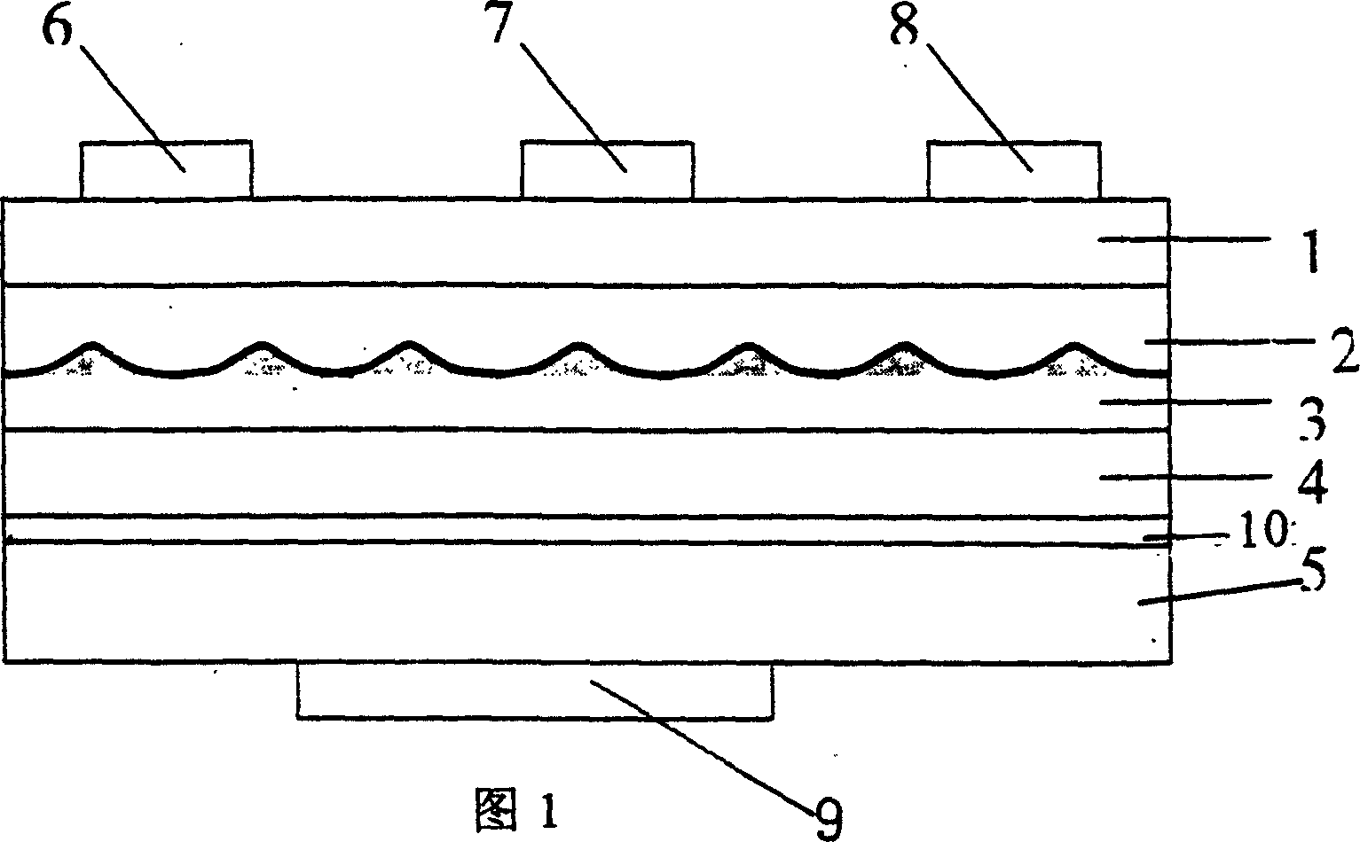
[0041] Referring to Figure 2 for the structure of the device produced in this embodiment, the structure of the device is grown by the molecular beam MBE method, and its structure will be described in detail in conjunction with the fabrication method of the device:

[0042] (a) Using Si-doped n + The (001) orientation GaAs is used as the substrate, and the device structure includes from bottom to top on the substrate: 2.0μm GaAs buffer layer, the substrate and buffer layer are 5; 70nm thick Al 0.3 Ga 0.7 As / GaAs superlattice barrier 10, where Al 0.3 Ga 0.7 As thickness is 5nm, GaAs is 2nm, a total of 10 periods; δ-Si doped layer 4, after doping carrier surface density is 3.8×10 11 cm 2 ; 4nm thick GaAs layer is the semiconductor isolation layer 3; Quantum dots are grown under the condition of substrate rotation, the amount of InAs deposited is 1.8ML, the substrate temperature for deposition is 440°C, the effective diameter of quantum dots is 12nm, and the density of quantu...

Embodiment 2

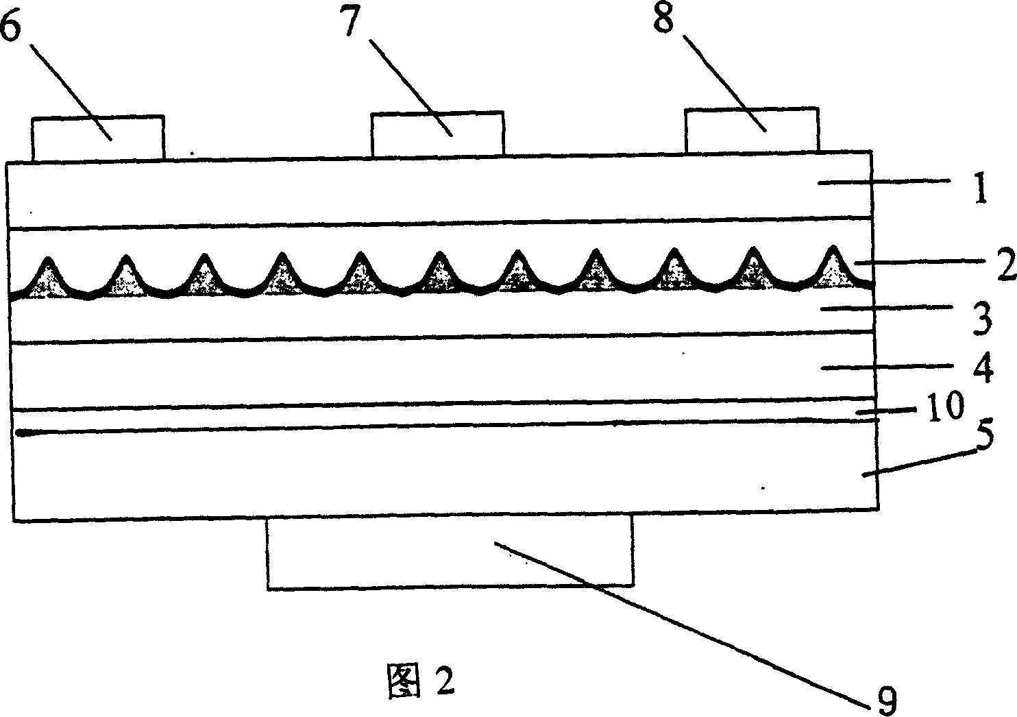
[0047] Referring to Figure 3 for the structure of the device produced in this embodiment, the structure of the device is grown by the molecular beam MBE method, and its structure is described in detail in conjunction with the fabrication method of the device:

[0048] (a) Using Si-doped n + The (001) orientation GaAs substrate, the device structure on the substrate from bottom to top includes: 1.0μm n + -GaAs buffer layer with a doping concentration of 1.0×10 18 cm -3 , the substrate and buffer layer are shown as 5 in Figure 3; the 700nm thick Al 0.3 Ga 0.7 As / GaAs superlattice barrier 10, where Al 0.3 Ga 0.7 The thickness of As is 5nm, GaAs is 2nm, a total of 100 periods; a layer of δ-Si doped layer 4, the surface density of carriers after doping is 4.8×10 11 cm -2 5nm thick GaAs semiconductor isolation layer 3; InAs quantum dot layer 2 with a thickness of 0.9 nanometers, and a 3nm thick GaAs capping layer, that is, the semiconductor capping layer 1. The quantum dots ...

Embodiment 3

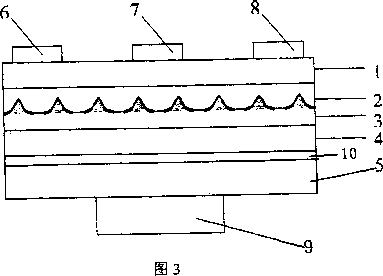
[0052] Referring to Figure 4 for the structure of the device produced in this embodiment, the structure of the device is grown by the molecular beam MBE method, and it is described in detail in conjunction with the manufacturing method of the device:

[0053] Si-doped n + The (001) orientation GaAs substrate, the device structure includes from bottom to top on the substrate: 2.0μm GaAs buffer layer; 70nm thick Al 0.3 Ga 0.7 As / GaAs superlattice barrier 10, where Al 0.3 Ga 0.7 As thickness is 5nm, GaAs is 2nm, a total of 10 periods; a layer of δ-Si doped layer 4, after doping carrier surface density is 1.4×10 11 cm -2 ; 4nm thick GaAs layer is the semiconductor isolation layer 3; Quantum dots are grown under the condition of substrate rotation, the deposition amount of InAs is 1.2ML, the substrate temperature of deposition is 400℃, the effective diameter of quantum dots is 15nm, and the density of quantum dots is 2.3×10 10 cm -2. After the device material is grown and t...


PUM

PropertyMeasurementUnit
Thicknessaaaaaaaaaa
Thicknessaaaaaaaaaa
Thicknessaaaaaaaaaa

Abstract

The invention discloses a composite quantum point device and a process for making it. The device includes a doping buffer layer made on the substrate using the high adulterated conductive GaAs in sequence by a molecular beam epitaxy method, semi-conductive GaAs isolating layer, an InAs quantum point layer and a thin GaAs cover layer covered on the InAs quantum point layer, an electrode prepared on the cover layer of the substrate and depositing AuGeNi on the back of the substrate as the back grid of the device, it also includes an AlGaAs/GaAs layer, a superlattice barrier layer prepared on the buffer layer and a theta -Si doping layer. The device is a composite quantum point device made by arrangement such as quantum points, two-dimensional gas and a thin Schottky barrier layer using the conventional method, it possesses a plurality of functions including luminescence, optical detection, amplification and storage.

Description

technical field [0001] The invention relates to microelectronic devices, optoelectronic devices and nanometer devices, in particular to a composite quantum dot device prepared by using a composite structure of quantum dots and two-dimensional electron gas and a preparation method. Background technique [0002] With the continuous improvement of the integration level of microelectronic devices, the scale of device units is getting smaller and smaller. When the size of the active region of the device reaches the range of 1 nanometer to 100 nanometers, the performance of the device and its working principle have great changes. Such devices are often referred to as nanodevices. At present, the recognized nano-devices are: (1) quantum dot devices, (2) single-electron devices and (3) resonant tunneling devices. Quantum dot devices are widely used in optical and electrical fields, such as quantum dot lasers, ideal single photon sources, single photon detectors and quantum dot mem...

Claims


Application Information

Patent Timeline
IPC IPC(8): B82B1/00B82B3/00H01L29/66H01L49/00
CPCB82Y10/00B82Y30/00
Inventor 竺云王太宏
Owner INST OF PHYSICS - CHINESE ACAD OF SCI
Why Eureka
Try Eureka