Method for manufacturing semiconductor device

A manufacturing method, semiconductor technology, applied in the direction of semiconductor/solid-state device manufacturing, semiconductor devices, electric solid-state devices, etc., can solve the problem of deteriorating tantalum oxide film step coverage, poor film quality capacitive insulating film, impossible to form capacitive insulating film, etc. question

Inactive Publication Date: 2004-01-28
PS4 LUXCO SARL
View PDF4 Cites 4 Cited by
  • Summary
  • Abstract
  • Description
  • Claims
  • Application Information

AI Technical Summary

Problems solved by technology

If oxygen vacancies are formed in the tantalum oxide film, there is a disadvantage that leakage current flows through the formed film, resulting in the formation of a capacitive insulating film with poor film quality
As a result, the step coverage of the formed tantalum oxide film is deteriorated, so that the film thickness of the capacitive insulating film formed on the surface of the lower electrode tends to be non-uniform, making it difficult to obtain stable capacitor capacitance when forming the capacitor.
In particular, when the lower electrode is a three-dimensional structure such as a cylinder, or forms the surface shape of the electrode like hemispherical silicon grains (HSG) in order to increase capacitance, the step coverage is significantly deteriorated, causing a problem that it is not possible to obtain The desired capacitance value, or the top and bottom electrodes are shorted to each other
Therefore, leakage current flows through the capacitor, making it difficult for the capacitor to function as an information storage capacitive element, resulting in deterioration of the reliability of the associated DRAM
In this case, in the method for producing a tantalum oxide thin film disclosed in the aforementioned Japanese Patent Application Laid-Open No. 2000-340559, if the heat treatment for introducing oxygen gas is prolonged to provide enough oxygen vacancies in the formed tantalum oxide thin film amount of oxygen, necessarily worsens yield
In addition, when the duration of heat treatment is extended, the surface such as polysilicon constituting the lower electrode is oxidized to form a silicon oxide film or the like with a smaller dielectric constant, thereby lowering the total capacitance value of the capacitor
[0014] With this conventional semiconductor device manufacturing method, it is impossible to form a capacitive insulating film with good step coverage and good film quality

Method used


Image

  • Method for manufacturing semiconductor device
  • Method for manufacturing semiconductor device
  • Method for manufacturing semiconductor device

Examples


no. 1 example

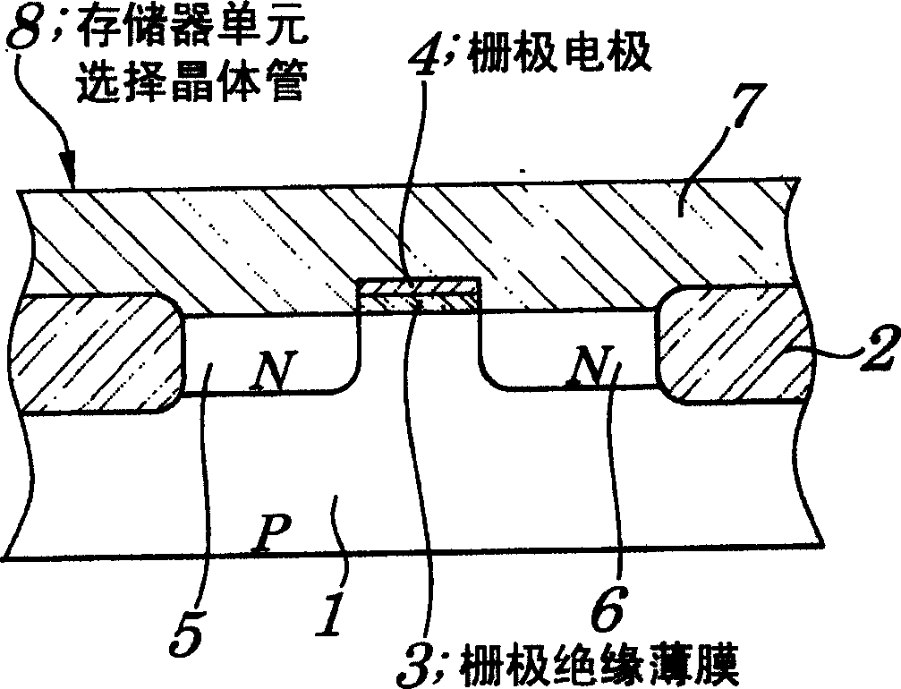
[0066] The following will refer to Figures 1A-1E and figure 2 , the method of manufacturing the semiconductor device according to the first embodiment will be described.

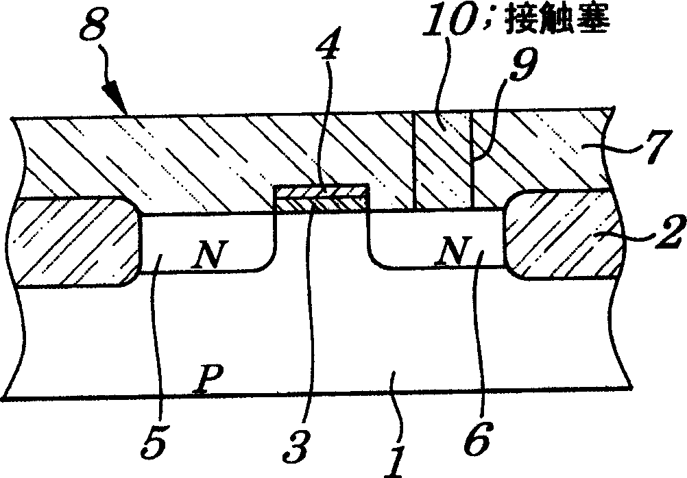
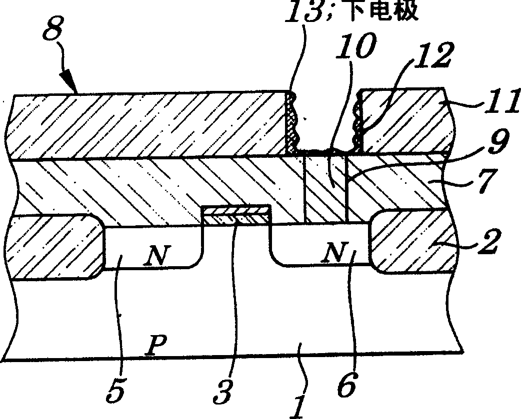
[0067] First, if Figure 1A As shown, for example, an element isolation region 2 is formed by using a P-type semiconductor substrate 1 by a known method such as LOCOS (Local Oxidation of Silicon) or STI (Shallow Trench Isolation), thereby forming an element isolation region 2 in the center of each active region. A gate insulating film 3 made of, for example, a silicon oxide film, and a gate electrode 4 made of, for example, a polysilicon film. Next, by utilizing self-alignment of the gate electrode 4, ions of N-type impurities are implanted to form a pair of N-type regions 5 and 6 respectively serving as source regions and drain regions; A first interlayer insulating film 7 composed of the same, to form a memory cell selection transistor 8 composed of an N-type MOS (NMOS) transistor.

[0068]Next, if ...

no. 2 example

[0078] The semiconductor device manufacturing method of this embodiment is very different in structure from the semiconductor device manufacturing method of the first embodiment, in which the two-stage deposition step ST described in the principle paragraph is repeated three times to finally form a tantalum oxide film, the oxide The tantalum film constitutes the capacitive insulating film and has a final desired film thickness (10 nm, the same value as that of the first embodiment). The following will refer to image 3 This semiconductor device manufacturing method is described.

[0079] That is, in the first embodiment Figure 1D in the process, according to image 3 A tantalum oxide film is formed in a sequence of depositions to form a capacitive insulating film 14 made of a tantalum oxide film on the lower electrode 13 .

[0080] With the structure of the second embodiment, the two-stage deposition step ST described in the principle paragraph was repeated three times to ...

no. 3 example

[0085] The structure of the semiconductor device manufacturing method of this embodiment is very different from the semiconductor device manufacturing method of the first embodiment, wherein when the two-stage deposition step ST is repeated twice to finally form a In the case of the same 10nm) tantalum oxide film, as described in the principle paragraph, at the first extreme S1 of each deposition step ST, in addition to the raw material gas, a small amount of oxygen is introduced. In this case, the amount of oxygen introduced in the first stage is chosen in such a way that the coverage is not deteriorated. The following will refer to Figure 4 A semiconductor device manufacturing method is described.

[0086] That is, in the first embodiment Figure 1D in the process, according to Figure 4 A tantalum oxide film is formed in a sequence of depositions to form a capacitive insulating film 14 made of a tantalum oxide film on the lower electrode 13 .

[0087] With the structur...


PUM

PropertyMeasurementUnit
thicknessaaaaaaaaaa
thicknessaaaaaaaaaa
thicknessaaaaaaaaaa

Abstract

There is provided a method for manufacturing a semiconductor device including a capacitor having a lower electrode, an upper electrode and a capacitive insulating film between the lower electrode and the upper electrode on a semiconductor substrate, wherein the capacitive insulating film is formed on the lower electrode over the semiconductor substrate using a chemical vapor deposition method, the method including: a lower electrode forming step of forming the lower electrode on the semiconductor, a dual-stage deposition step including a first stage for introducing a material gas containing a specified metal into a reactor in which the semiconductor substrate is placed and a second stage for subsequently introducing an oxidizing gas into the reactor, and wherein a metal oxide film as an oxide of the specified metal is formed on the lower electrode over the semiconductor substrate, by repeating the dual-stage deposition step two or more times, thereby forming the capacitive insulating film; and an upper electrode forming step of forming the upper electrode on the capacitive insulating film. Thus, it is possible to obtain the capacitive insulating film having good step coverage and a good film quality, without reducing throughput.

Description

[0001] This application claims priority from Japanese Patent Application No. 2002-194006 filed on July 2, 2002, which is incorporated herein by reference. technical field [0002] The present invention relates to a method of manufacturing a semiconductor device, in particular, to a method of manufacturing a semiconductor device having a capacitor (information storage capacitance element), utilizing such as tantalum oxide (Ta 2 o 5 ) film and other metal oxide films are used as capacitive insulating films to form the capacitor. Background technique [0003] Large scale integration (LSI), which is considered to be representative of semiconductor devices, is roughly divided into memory products and logic products, among which memory products in particular have been remarkably developed along with the development of semiconductor device manufacturing technology in recent years. In addition, memory products are divided into dynamic random access memory (DRAM) and static random a...

Claims


Application Information

Patent Timeline
Patent Type & Authority Applications(China)
IPC IPC(8): C23C16/44C23C16/40C23C16/455G11C7/00H01L21/02H01L21/205H01L21/316H01L21/8242H01L27/108
CPCC23C16/45553H01L21/31637H01L28/40H01L27/10852C23C16/405H01L21/02183H01L21/0228H01L21/02189H01L21/02181H10B12/033H10B99/00
Inventor 藤冈弘文小柳贤一
Owner PS4 LUXCO SARL
Why Eureka
Try Eureka