

Method of mfg. GaN-base LED
A technology of light-emitting diodes and manufacturing methods, which is applied to electrical components, circuits, semiconductor devices, etc., and can solve problems such as difficulty in finding heat sink materials, unfavorable luminous efficiency and thermal stability of devices, etc.
- Summary
- Abstract
- Description
- Claims
- Application Information
AI Technical Summary
Problems solved by technology
Method used
Image

Examples
Embodiment 1
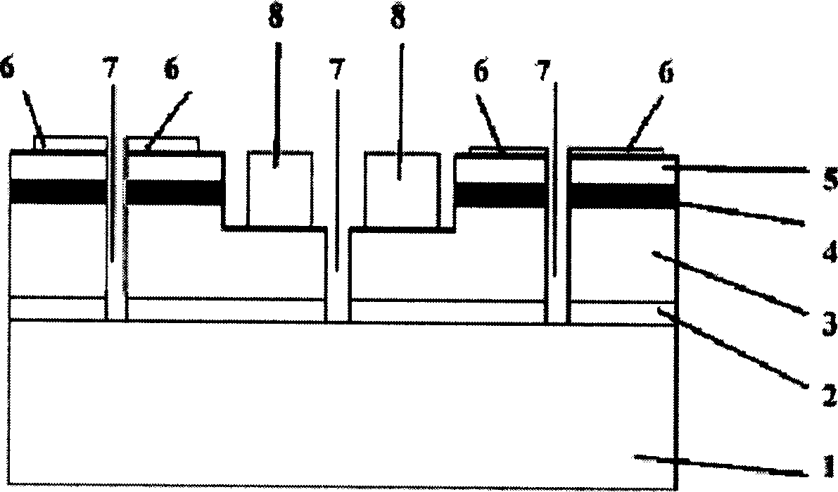
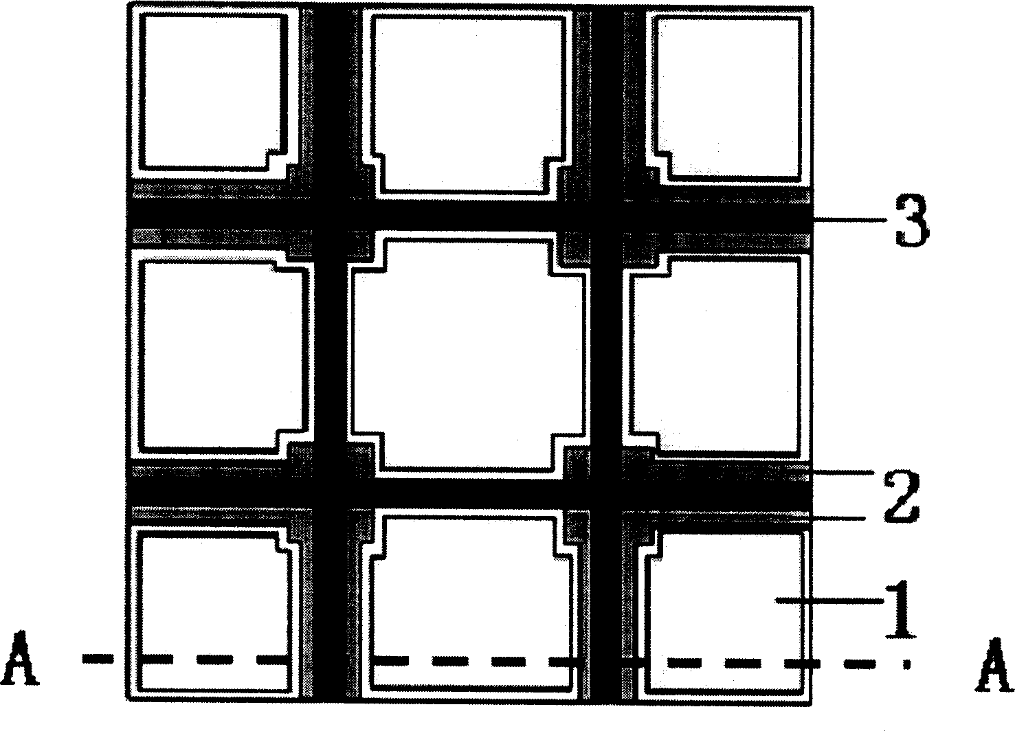
[0033] The basic structure of the material of the grid-shaped small-size light-emitting area light-emitting diode based on gallium nitride material disclosed by the present invention is as follows: figure 1 As shown, its light-emitting area graphics, such as figure 2 Shown: 1 is the p-electrode, 2 is the n-electrode, and 3 is the etched deep groove. The profile obtained along AA is as follows image 3 Shown: 1 is sapphire substrate, 2 is buffer layer, 3 is n-type GaN, 4 is active area, 5 is p-type GaN, 6 is p-type electrode, 7 is n-type electrode, 8 is etched deep grooves.
[0034] When making the device, deep grooves are etched between different small-scale light-emitting regions in the chip, and the deep grooves of the well-shaped pattern are obtained by dry etching or wet etching, so that the isolation between each light-emitting region is achieved, thereby reducing the The thermal strain caused by the mismatch of the thermal expansion coefficient between the substrate ...
Embodiment 2
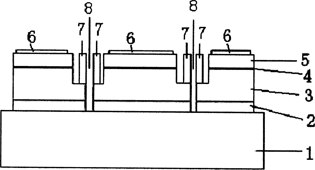
[0037] The basic structure of the material of the P-shaped small-size light-emitting area light-emitting diode based on gallium nitride material disclosed by the present invention is as follows: figure 1 As shown, only its light-emitting area graphics, such as Figure 4 Shown: 1 is the p-electrode, 2 is the n-electrode, and 3 is the etched deep groove. When making the device, deep grooves are etched between different small-scale light-emitting regions in the chip, and the deep grooves isolated by the Pozi pattern are obtained by dry etching or wet etching, so that the isolation between each light-emitting region is achieved, thereby Reduce the thermal stress caused by the thermal expansion coefficient mismatch between the substrate material and the epitaxial chip, and obtain a GaN-based light-emitting diode with uniform, stable and reliable light emission under high current injection. Experiments have proved that the stability of the high-power GaN-based light-emitting diode ...
Embodiment 3
[0040] GaN-based light-emitting diodes disclosed in the present invention such as Figure 5 As shown, 1 is the heat sink material diamond, 2 is the p-electrode on the heat sink substrate, 3 is the welding electrode, 4 is the p-electrode of the chip, 5 is the p-type gallium nitride, 6 is the active region, and 7 is the n-type nitrogen Gallium chloride, 8 is the buffer layer, 9 is the ZnO substrate, 10 is the etched deep groove, 11 is the n-electrode of the chip, and 12 is the n-electrode on the heat sink substrate. By etching deep grooves between different small-scale light-emitting areas in the chip, small well-shaped or rice-shaped light-emitting areas are formed, so that the isolation between each light-emitting area is achieved, and the GaN-based epitaxial wafer is connected to the high-heat The thermal conductivity of the heat sink material 1 is welded, and the temperature of the chip itself is reduced through the efficient heat conduction of the high thermal conductivity ...
PUM
| Property | Measurement | Unit |
|---|---|---|
| Width | aaaaa | aaaaa |
Abstract
Description
Claims
Application Information