

Electrochemical deep etching method and apparatus thereof
A deep etching and electrochemical technology, which is applied in the field of microelectronics and microelectromechanical systems, can solve problems such as lateral erosion and structural collapse, and achieve the effects of less chemical reagents, reduced lateral erosion, and low operating costs
- Summary
- Abstract
- Description
- Claims
- Application Information
AI Technical Summary
Problems solved by technology
Method used
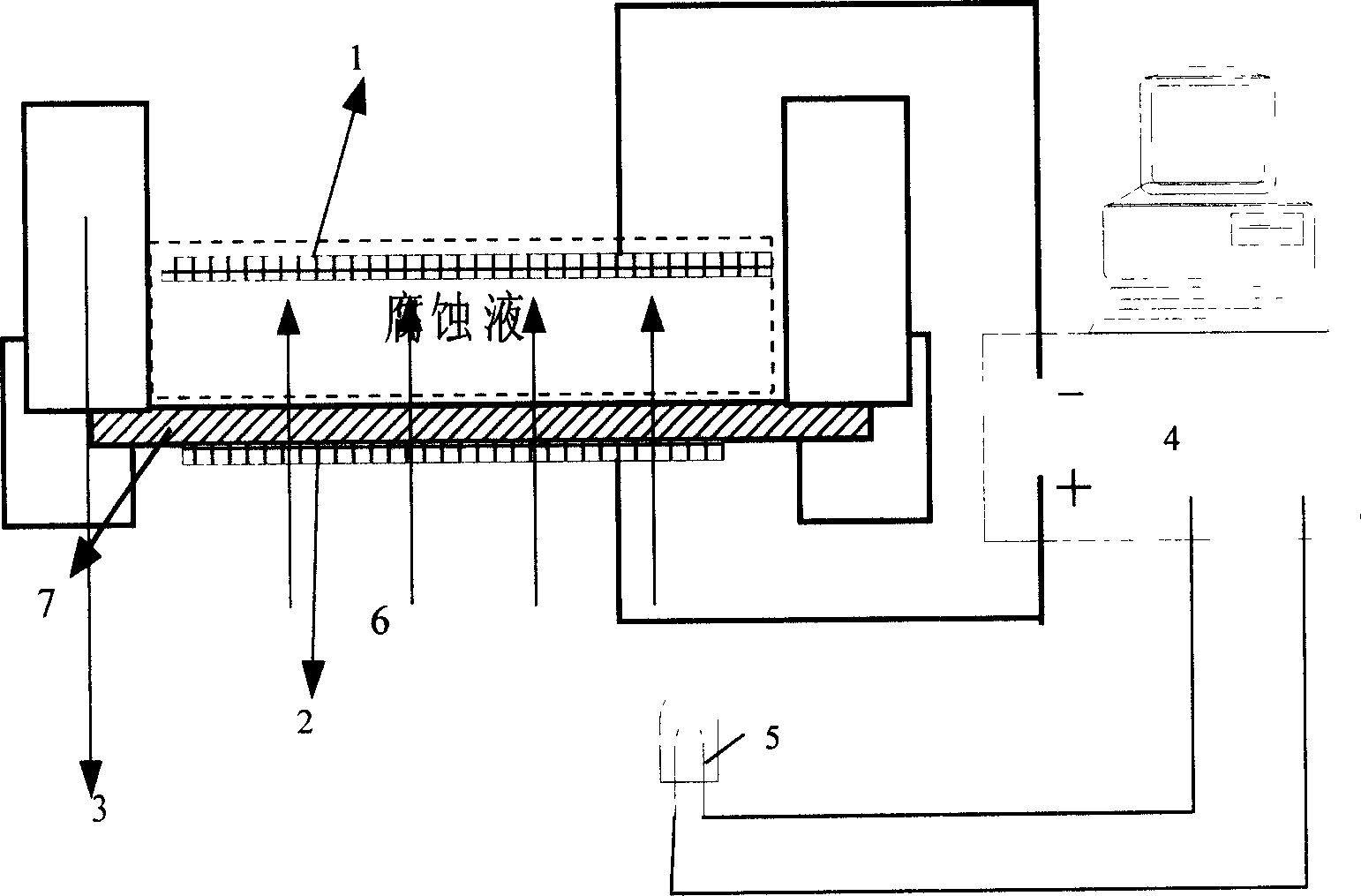
Image

Examples
Embodiment 1
[0021] Example 1: Fabrication of Silicon Precision Interdigital Capacitors
[0022] Silicon interdigitated capacitors are an important part of silicon inertial gyroscopes. Using high aspect ratio deep etching technology can shorten interdigital spacing, increase effective capacitance, and improve resolution. Here is an electrochemical deep etching method to make this kind of interdigitated capacitor. The layout design of the device needs to consider the size of the interdigitated capacitor. If the spacing is greater than 2 microns, it is recommended to use a method of combining small structures. In this embodiment, the spacing is 1 micron, the process steps are as follows:
[0023] The sample used in this embodiment is a silicon wafer, and the silicon wafer is an n-type silicon wafer with a resistivity of 1-5Ω·cm.
[0024] 1. Firstly, As ions are used to implant the back surface with a dose of 5×10 15 / cm 2 , the energy can be selected as 150keV, and then activated by anne...
Embodiment 2
[0032] Example 2: Silicon micro-nano channel
[0033] Making micro-nano channels through up and down on silicon wafers has many uses. It can be made into micro-channel photomultiplier devices, and can also be made into filters specially used in nanobiology, such as DNA filters. In addition, it can also be As the central channel of the micro-nano needle, it is similar to Example 1. Note that if the channel density is relatively large, the requirements for the mask layer are not high, and ordinary materials such as silicon nitride, silicon carbide, and gold-chromium alloy can be used. Specifically, In terms of the fabrication of the silicon micro-nano channel in this embodiment, the silicon micro-nano channel is 0.5 μm, and the sample is also a silicon chip, and the sample silicon in Example 1 is an n-type silicon chip, and its resistivity is 1-5Ω cm, the process steps are as follows:
[0034] 1. First, As or P ions are used to implant the back surface with a dose of 5×10 15 / ...
PUM
| Property | Measurement | Unit |
|---|---|---|
| magnetic flux density | aaaaa | aaaaa |
| width | aaaaa | aaaaa |
| electrical resistivity | aaaaa | aaaaa |
Abstract
Description
Claims
Application Information