Plasma etching method for eliminating organic substance using sulfur dioxide mixture gas

A technology of sulfur dioxide and mixed gas, which is applied in the manufacture of electrical components, semiconductor/solid-state devices, circuits, etc., can solve problems affecting circuit performance and structural differences, and achieve the effects of eliminating time delays of resistors and capacitors, improving impacts, and increasing yields

Inactive Publication Date: 2005-06-29
SHANGHAI HUA HONG GROUP +1
View PDF0 Cites 1 Cited by
  • Summary
  • Abstract
  • Description
  • Claims
  • Application Information

AI Technical Summary

Problems solved by technology

Compared with the commonly used method of using fluorocarbon etching gas to remove organic matter in the industry, while etching organic matter, it will etch the underlying oxide or low-dielectric material, resulting in a difference in structure (micro-loading effect) , which ultimately affects circuit performance

Method used


Image

  • Plasma etching method for eliminating organic substance using sulfur dioxide mixture gas
  • Plasma etching method for eliminating organic substance using sulfur dioxide mixture gas
  • Plasma etching method for eliminating organic substance using sulfur dioxide mixture gas

Examples


Embodiment Construction

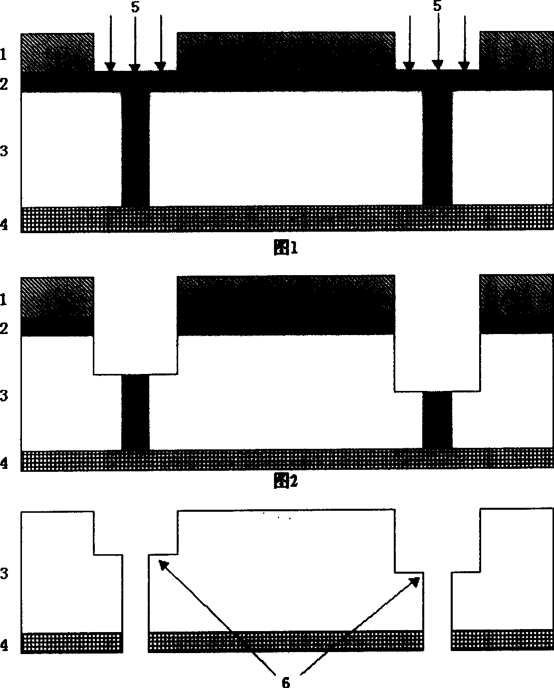
[0015] Implementation steps of the present invention are as follows:

[0016] 1. Deposit the etching barrier material by enhanced plasma chemical vapor deposition: silicon carbide;

[0017] 2. Deposit insulating dielectric material by enhanced plasma chemical vapor deposition method: silicon dioxide:

[0018] 3. Carry out the first photolithography step to expose the pattern of the through hole on the silicon wafer;

[0019] 4. Etching the through hole, removing the photoresist, and cleaning the silicon wafer;

[0020] 5. Filling and coating of organic matter in the anti-reflection layer;

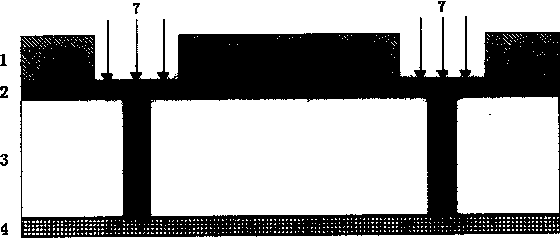
[0021] 6. Carry out the second photolithography step to expose the pattern of the metal groove on the silicon wafer;

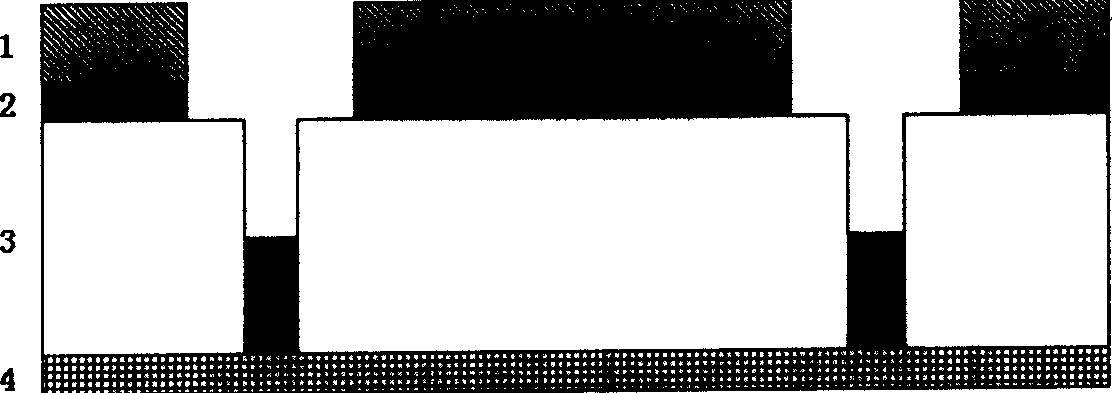
[0022] 7. Use sulfur dioxide mixed gas, the mixed gas can be oxygen, hydrogen, nitrogen, argon, carbon monoxide, carbon dioxide or fluorocarbon gas, the volume ratio of sulfur dioxide to mixed gas is 0.5:1 or 1.25:1 or 3:1, for The organic filling layer is etched;

[0...


PUM


Abstract

This invention relates to plasm etching process to eliminate the micro-loading effect in the damascene structure in the integration copper channel. The dual damascene technique is the new metal distribution technique with the development of the deep micron integration technique.

Description

technical field [0001] The invention belongs to the technical field of integrated circuit technology, and in particular relates to a plasma etching method for eliminating organic matter in an integrated circuit by using sulfur dioxide mixed gas. Background technique [0002] With the continuous development of information technology, communication technology and Internet technology, the requirements for integrated circuit performance are getting higher and higher, which in turn promotes the rapid development of integrated circuit manufacturing technology in the direction of high integration, large capacity, high speed and low power consumption. . As the chip runs faster and faster, how to maintain low power consumption and low heat generation, prolong the use time, and maximize the overall performance of the chip has become one of the keys to integrated circuit manufacturing. [0003] The conduction of integrated circuits is accomplished by metal wiring. In the past, metal a...

Claims


Application Information

Patent Timeline
Patent Type & Authority Applications(China)
IPC IPC(8): H01L21/3065H01L21/311
Inventor 周炜捷
Owner SHANGHAI HUA HONG GROUP
Why Eureka
Try Eureka