Photovoltaic device

A photoelectric conversion device, transparent electrode technology, applied in photovoltaic power generation, circuits, electrical components and other directions, can solve problems such as neglect

Inactive Publication Date: 2005-07-13
MITSUBISHI HEAVY IND LTD
View PDF1 Cites 17 Cited by
  • Summary
  • Abstract
  • Description
  • Claims
  • Application Information

AI Technical Summary

Problems solved by technology

That is, the amount of Ga addition was studied in order to improve the photoelectric conversion efficiency without paying attention to the effect on the Ga-added Si layer (p layer or n layer) / ZnO:Ga interface characteristics, ZnO:Ga resistivity or transmittance. , there is still room for improving the photoelectric conversion efficiency

Method used


Image

  • Photovoltaic device
  • Photovoltaic device
  • Photovoltaic device

Examples


no. 1 approach

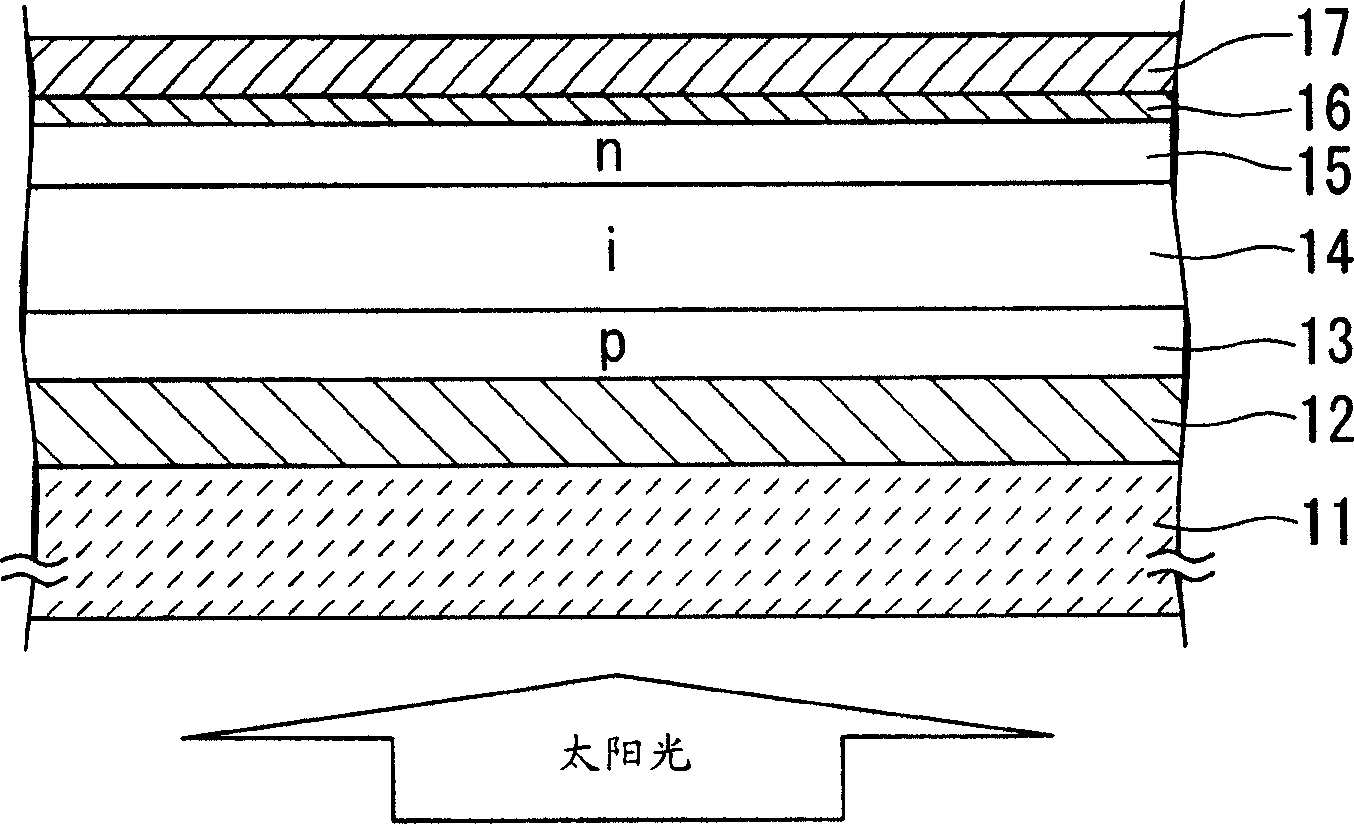
[0059] Below, refer to figure 1 A photoelectric conversion device according to a first embodiment of the present invention will be described.

[0060] The photoelectric conversion device of the present embodiment is of a type in which light is incident on a transparent insulating substrate, and its power generation layer is made of microcrystalline silicon.

[0061] (first process)

[0062] The first transparent electrode 12 is formed on the transparent insulating substrate 11 . On the transparent insulating substrate 11 , for example, white glass is used to indicate light transmission.

[0063] Ga (gallium)-added ZnO (zinc oxide) was used as the first transparent electrode 12 . In addition, it is preferable to form a reduction prevention film on the first transparent electrode 12 .

[0064] The transparent insulating substrate 11 was set in a DC spray coating apparatus, and a Ga-added ZnO film was formed on the transparent insulating substrate 11 by DC spray coating in a ...

no. 2 approach

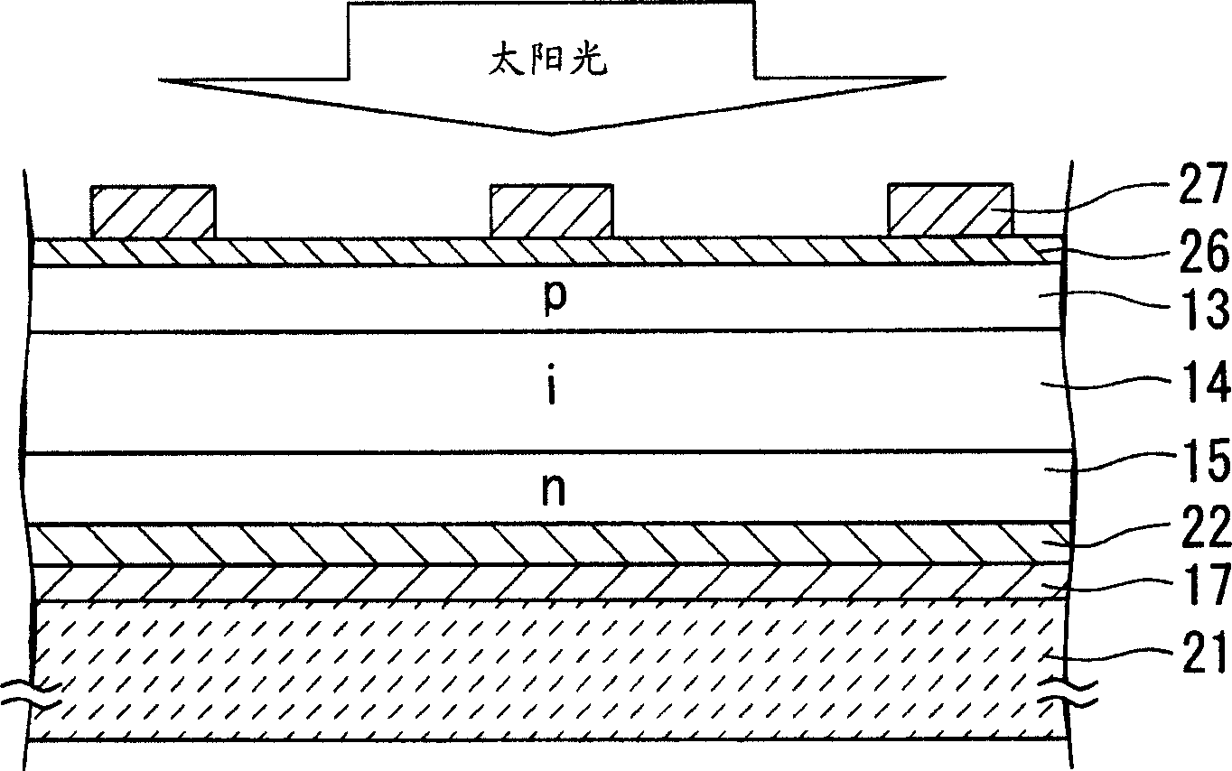
[0092] Below, refer to figure 2 A photoelectric conversion device according to a second embodiment of the present invention will be described.

[0093] The photoelectric conversion device of this embodiment is the same as that of the first embodiment in that the power generation layer is formed of microcrystalline silicon; the difference from the first embodiment is that it is also applicable when the insulating substrate is opaque, and that the light is transmitted from the collector in the opposite direction. Type of side incidence.

[0094] (first process)

[0095] The backside electrode 17 and the first transparent electrode 22 are formed on an opaque insulating substrate 21 that does not transmit light. For the opaque insulating substrate 21, for example, a stainless steel plate is used. Meanwhile, instead of the opaque insulating substrate 21 , soda glass (blue plate (blue plate)) may be used.

[0096] Ag or Al is used as the backside electrode 17 . As in the first...

no. 3 approach

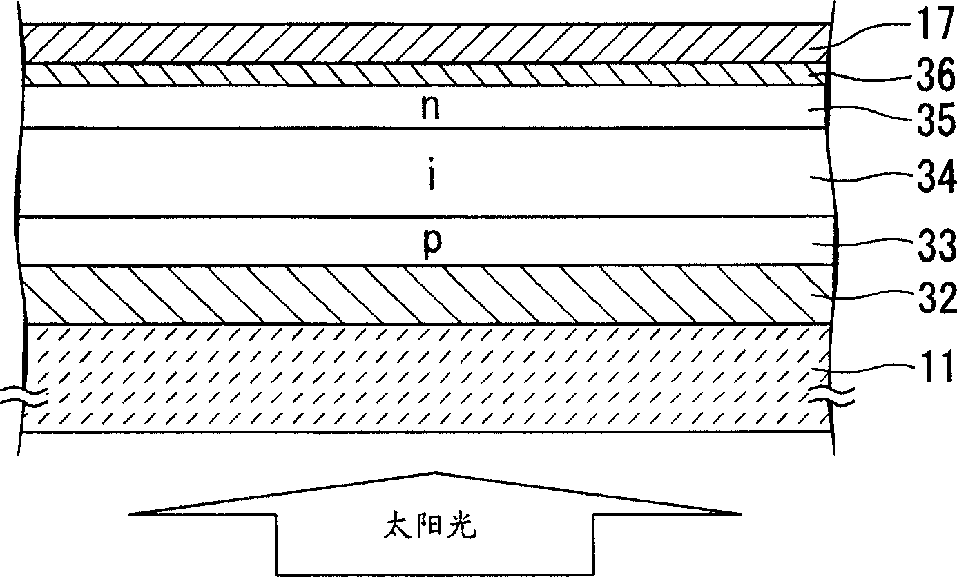
[0112] Below, refer to image 3 A photoelectric conversion device according to a third embodiment of the present invention will be described.

[0113] The photoelectric conversion device of this embodiment differs from the first and second embodiments in that the power generation layer is formed of amorphous silicon, and is of the same type as the first embodiment in that light is incident on a transparent insulating substrate.

[0114] (first process)

[0115] The first transparent electrode 32 is formed on the transparent insulating substrate 11 . On the transparent insulating substrate 11 , for example, white glass is used to indicate light transmission.

[0116] Using SnO 2 (tin dioxide) as the first transparent electrode 32 .

[0117] Set the transparent insulating substrate 11 in the atmospheric pressure thermal CVD device, with SnCl 4 , water vapor (H 2 O), hydrogen fluoride (HF) as raw materials to form SnO on the transparent insulating substrate 11 2 .

[0118...


PUM


Abstract

A photoelectric conversion device that achieves a high photoelectric conversion rate using a transparent electrode or a transparent conductive film having an optimal relationship between resistivity and transmittance. On the transparent insulating substrate, there are at least sequentially stacked: a first transparent electrode, a pin structure or a nip structure microcrystalline silicon layer composed of a p-type silicon layer, an i-type silicon layer and an n-type silicon layer, a second transparent electrode and The backside electrode, wherein at least one of the first transparent electrode and the second transparent electrode is a Ga-added ZnO layer, and the content of Ga is less than or equal to 15 atomic % relative to Zn.

Description

technical field [0001] The present invention relates to a photoelectric conversion device whose transparent electrode is ZnO (zinc oxide). Background technique [0002] Conventionally, silicon-based thin-film photoelectric conversion devices have been known as photoelectric conversion devices such as solar cells. Usually, a first transparent electrode, a silicon-based semiconductor layer (photoelectric conversion layer), a second transparent electrode, and a metal electrode film are laminated in this order on the substrate of the photoelectric conversion device. [0003] As a transparent electrode, a material with low resistance and high light transmittance is required, so ZnO (zinc oxide), SnO 2 (tin dioxide) and so on. [0004] The low resistance of such a transparent electrode is achieved by adding Ga (gallium) oxide, Al (aluminum) oxide, fluorine, or the like. [0005] In addition, when an amorphous silicon thin film is used as a photoelectric conversion layer, there ...

Claims


Application Information

Patent Timeline
Patent Type & Authority Applications(China)
IPC IPC(8): H01L21/28H01L31/0224H01L31/04H01L31/075H01L31/076H01L31/077
CPCH01L31/022483H01L31/075H01L31/076H01L31/1884Y02E10/547Y02E10/548
Inventor 渡辺俊哉山下信树中野要治吴屋真之坂井智嗣米仓义道
Owner MITSUBISHI HEAVY IND LTD
Why Eureka
Try Eureka