Color filter materials, color filters, manufacturing method and image sensor
A color filter and dye technology, applied in the field of color filter materials, can solve problems such as insufficient curing, thinning of image sensors, and obstacles to miniaturization and high sensitivity
- Summary
- Abstract
- Description
- Claims
- Application Information
AI Technical Summary
Problems solved by technology
Method used
Image

Examples
Embodiment approach 1
[0035] The color filter material of the present invention is a color filter material containing a dye with photosensitive function, and the photosensitive curing reaction may be any one of radical polymerization, cationic polymerization, and anionic polymerization.
[0036] As an example of a material when radical polymerization is used, an acrylic compound in which an acryloyl group is added to the dye R can be used, that is:
[0037] R-CO-CH=CH 2 Or compounds with adducted methacryloyl groups, namely:
[0038] R—CO—C(CH3)=CH2 In addition, compounds having maleimide groups and enthiol compounds can be used for non-acrylic systems.
[0039] When light is irradiated to the color filter material containing the photosensitive function added dye and the photocuring initiator, the photosensitive function added dye forms a radical state, and a chain reaction of polymerization progresses to cure. That is, a dye-containing polymer can be obtained without using a binder.
[0040] In...
Embodiment approach 2
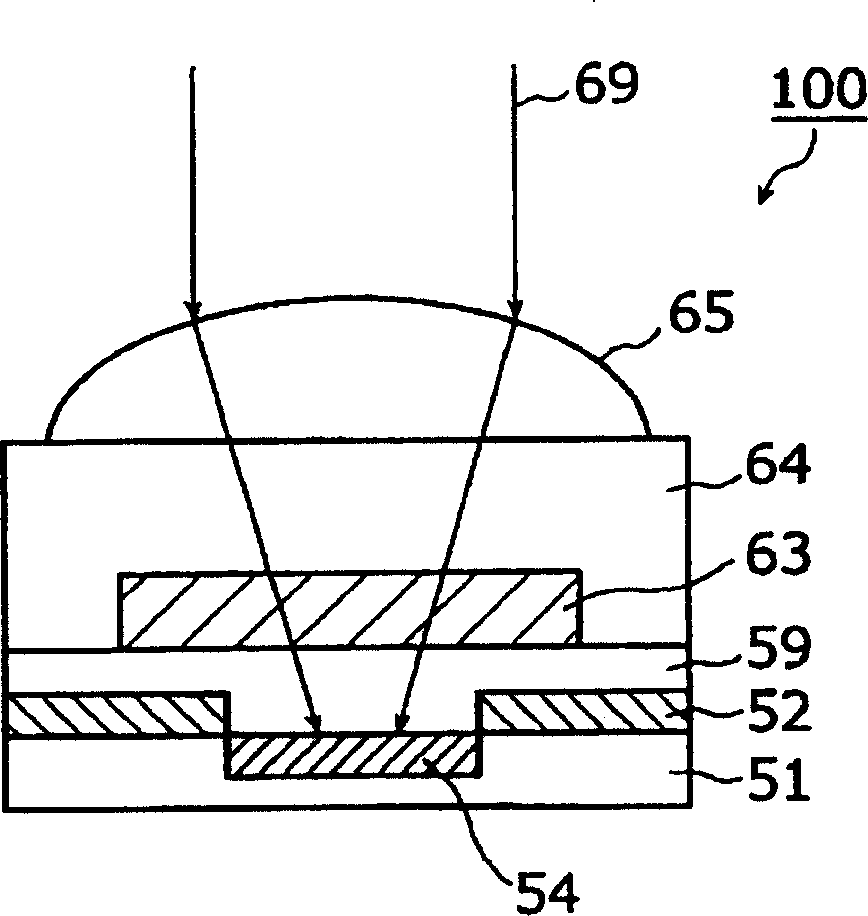
[0046] figure 1 It is a cross-sectional view of a unit pixel of an image sensor according to Embodiment 2 of the present invention. Such as figure 1 As shown, the unit pixel 100 according to the second embodiment includes a semiconductor substrate 51, a photodiode 54, a layer 52 including a light-shielding film and wiring, a transparent film 59 for planarization, and a color filter 63 according to the present invention. , a transparent planarizing film 64 and a single-chip microlens 65 for collecting incident light.
[0047] In the image sensor, a plurality of photodiodes 54 are formed in a matrix at equal intervals on a semiconductor substrate 51 . The photodiode 54 generates a signal charge which has the following figure 1 The amount of charge corresponding to the intensity of the light reaching the photodiode 54 among the light 69 incident from above. In addition, a layer 52 including a light-shielding film, wiring, and the like is formed to cover between the plurality ...
Embodiment approach 3
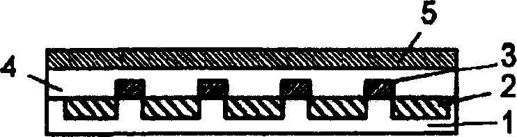
[0055] Figure 3A ~ Figure 3I It is a figure explaining the manufacturing method of the color filter concerning Embodiment 3 of this invention. Here, a method of manufacturing color filters of three types (RGB) for an image sensor will be described as an example.
[0056] Such as Figure 3A As shown, on the upper part of the semiconductor substrate 1 where the light receiving part (photodiode) 2 is formed, a layer 3 containing wiring etc. is formed so as to avoid the opening of the light receiving part 2, and a flat layer (transparent film) is formed on the upper part. )4. Thereafter, the material 5 for the first color filter of the present invention is spin-coated on top of the flat layer 4 . Secondly, if Figure 3B As shown, a photomask 8 defining a formation region of the first color filter is set on the upper portion thereof, and the pattern is exposed by irradiation with ultraviolet rays (i-ray) from above. Thus, only the first color filter material 5 in a predetermi...
PUM
 Abstract
Description
Claims
Application Information