Self-aligning silicide method for RF lateral diffusion field-effect transistor

A field-effect transistor and self-aligned silicide technology, which is used in semiconductor/solid-state device manufacturing, electrical components, circuits, etc., can solve the problem of large series resistance in source and drain regions, lack of design flexibility, and difficult self-aligned silicide in LDMOS. And other issues

Inactive Publication Date: 2005-11-02
INST OF MICROELECTRONICS CHINESE ACAD OF SCI
View PDF0 Cites 18 Cited by
  • Summary
  • Abstract
  • Description
  • Claims
  • Application Information

AI Technical Summary

Problems solved by technology

[0003] However, due to the existence of lightly doped drift regions, conventional LDMOS is difficult to realize self-aligned silicide, and there is a large series resistance in the source and drain regions, which limits the further improvement of radio frequency performance.
In order to realize self-aligned silicide, Satoshi Matsumoto et al. proposed a method of using a single-layer silicon dioxide sidewall to define the length of the drift region and rea

Method used


Image

  • Self-aligning silicide method for RF lateral diffusion field-effect transistor

Examples


Embodiment Construction

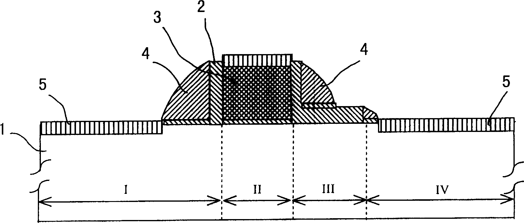
[0029] A self-aligned silicide method for radio frequency lateral diffusion field effect transistors of the present invention comprises the following steps:

[0030] Step 1: On the silicon wafer, perform maskless drift region implantation after polycrystalline gate etching;

[0031] Step 2: Deposit a thin layer of silicon dioxide by thermal decomposition of ethyl orthosilicate; this step 2 uses the thermal decomposition of ethyl orthosilicate to deposit silicon dioxide, and its thickness is 40-80nm;

[0032] Step 3: Protect the drift region with photoresist, etch silicon dioxide back, and form a silicon dioxide sidewall near the source side of the gate; this step 3 uses a photolithography plate to protect the drift region, and etches the silicon dioxide sidewall conditions For: power 400W, pore 1.2cm, argon 300sccm, carbon tetrafluoride 15sccm, trifluoromethane 35sccm, overcut 30%, endpoint trigger control;

[0033] Step 4: Source-drain self-alignment injection and deglue; in...


PUM

PropertyMeasurementUnit
Thicknessaaaaaaaaaa
Thicknessaaaaaaaaaa
Thicknessaaaaaaaaaa

Abstract

A method for radio frequency lateral diffusing self-alignment silicides of the field-effect-transistor, comprising the steps of: on the silicon chips, injecting the etched multiple crystal grids to the drifting zone without mask; depositing a thin silicon dioxide layer with tetraethylorthosilicate heat decomposition method; protecting drifting zone with photo resist and resisting silicon dioxide, forming a silicon dioxide sidewall on the gate side nearby the source; source-drain self-aligning injection and striping; quick heat annealing to eliminate injection damage and activate impurity; separately depositing a thin pad silicon dioxide with tetraethylorthosilicate heat decomposition method and depositing a silicon nitride with low pressure chemical vapour deposition method; sequentially resisting silicon nitride and silicon dioxide, forming a silicon nitride secondary sidewall on the silicon dioxide primary sidewall; sputtering a thin titanium layer; quick heat annealing to form the titanium silicides from the silicon and titanium; etching and removing the rest titanium; quick heat annealing to forming low resistance titanium silicides from high resistance ones.

Description

technical field [0001] The invention belongs to the technical field of semiconductors, in particular to a novel self-aligned silicide method for a radio frequency lateral diffusion field effect transistor (LDMOS). Background technique [0002] LDMOS has excellent radio frequency performance (large linear dynamic range, high linear gain, large output power, high power density, etc.), compared with gallium arsenide technology, which is the mainstream radio frequency process, it has low cost, simple process, mature and compatible with complementary metal - Advantages of the oxide-semiconductor (CMOS) process. At present, it is widely used in radio frequency power amplifiers (below 2GHz), and has become the mainstream of power devices in mobile communication base station power amplifiers, and plays an increasingly important role in terminal power amplifiers. [0003] However, due to the existence of the lightly doped drift region, it is difficult to realize self-aligned silicid...

Claims


Application Information

Patent Timeline
IPC IPC(8): H01L21/336
Inventor 杨荣李俊峰海潮和徐秋霞韩郑生柴淑敏赵玉印周锁京钱鹤
Owner INST OF MICROELECTRONICS CHINESE ACAD OF SCI
Why Eureka
Try Eureka