

Low temp polycrystal silicon film transistor and manufacturing method thereof
A thin-film transistor and low-temperature polysilicon technology, which is applied in the manufacture of transistors, semiconductor/solid-state devices, electrical components, etc., can solve the problems of high manufacturing cost of low-temperature polysilicon thin-film transistors, complicated LDD process, etc. The effect of low leakage current
- Summary
- Abstract
- Description
- Claims
- Application Information
AI Technical Summary
Problems solved by technology
Method used
Image

Examples
no. 1 example
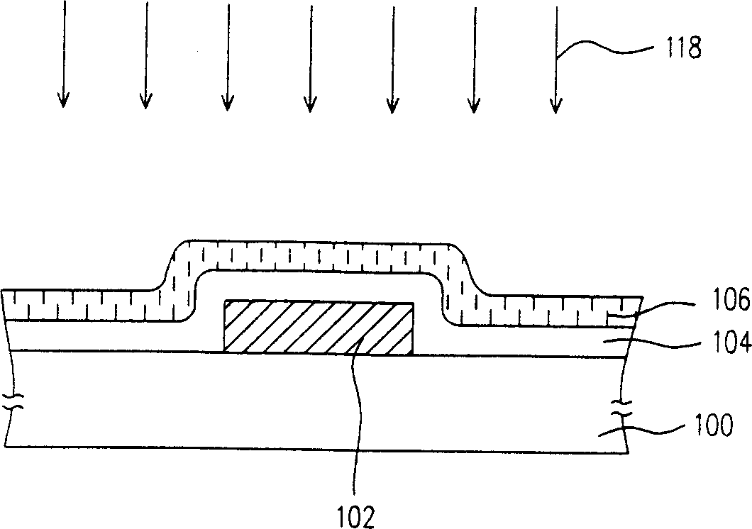
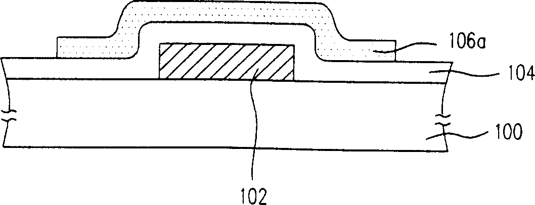
[0031] Figure 2A to Figure 2H Shown is a schematic cross-sectional view of the manufacturing process of a low-temperature polysilicon thin film transistor according to a preferred embodiment of the present invention. Please refer to Figure 2A Firstly, the gate electrode 202 , the gate dielectric layer 204 , the first amorphous silicon layer 206 and the patterned insulating layer 208 are sequentially formed on the substrate 200 . Wherein, the patterned insulating layer 208 is disposed on the first amorphous silicon layer 206 and located above the gate 202 . In this embodiment, the material of the patterned insulating layer 208 is, for example, silicon oxide or silicon nitride.
[0032] Please refer to Figure 2B , using the patterned insulating layer 208 as a mask to perform a doping process, such as performing an ion implantation process, to dope dopant ions 230 into the part of the first amorphous silicon layer 206 not covered by the patterned insulating layer 208 In or...
no. 2 example
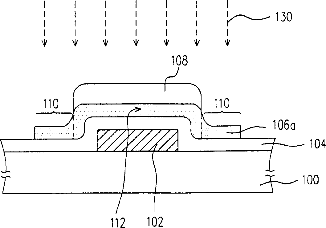
[0042] Figure 3A to Figure 3C Shown is a schematic cross-sectional schematic diagram of part of the manufacturing process of a low-temperature polysilicon thin film transistor according to another embodiment of the present invention. Please refer to Figure 3A , according to the above Figure 2A to Figure 2D After the first patterned amorphous silicon layer 206a and the second patterned amorphous silicon layer 210a are completed, the source / drain layer is then formed on the substrate 200 and the second patterned amorphous silicon layer 210a 218. Here, the second patterned amorphous silicon layer 210a is an ohmic contact layer serving as a thin film transistor.
[0043] Please refer to Figure 3B , and then irradiated with, for example, an excimer laser beam 222 Figure 3A The completed structure is such that part of the first patterned amorphous silicon layer 206a located above the gate 202 is melted and recrystallized to form a polysilicon channel region 212, as Figur...
no. 3 example
[0046] Figure 4A to Figure 4B Shown is a cross-sectional view of part of the manufacturing process of a low-temperature polysilicon thin film transistor according to yet another embodiment of the present invention. Please refer to Figure 4A ,according to Figure 2A After the patterned insulating layer 208 is formed on the substrate 200 according to the above process, a second amorphous silicon layer 310 is formed on the first amorphous silicon layer 206 to cover the patterned insulating layer 208 . Wherein, the second amorphous silicon layer 310 may be an amorphous silicon layer with or without dopants.
[0047] Please refer to Figure 4B , followed by Figure 2D As described above, the first patterned amorphous silicon layer 206 a and the second patterned amorphous silicon layer 310 a are formed. Then, a doping process is performed by using the patterned insulating layer 208 as a mask to dope dopant ions 230 into part of the first patterned amorphous silicon layer 206a...
PUM
 Abstract
Description
Claims
Application Information