

Polishing compound and method for polishing substrate
A polishing agent and substrate technology, applied in polishing compositions containing abrasives, chemical instruments and methods, inorganic chemistry, etc., can solve the problems of reduced polishing speed, inability to visually detect the degree of sedimentation, and unstable dispersion. , to achieve the effect of easy process management
- Summary
- Abstract
- Description
- Claims
- Application Information
AI Technical Summary
Problems solved by technology
Method used
Image

Examples
Embodiment 1
[0116] (Preparation of polishing compound)
[0117] 430 g Ce(NH 4 ) 2 (NO 3 ) 6 It was dissolved in 7300 g of pure water, and 240 g of ammonia water (25% aqueous solution) was mixed and stirred in this solution to obtain a suspension containing 160 g of cerium hydroxide (yellow-white). The obtained cerium hydroxide suspension was subjected to centrifugation (4000 rpm, 5 minutes) for solid-liquid separation, and fresh pure water was added after the liquid was removed. Centrifugation was then carried out under the above conditions, and this operation was repeated four times before washing. The specific surface area of the obtained particles was measured by the BET method and was 200 m2 / g. 160 g of the particles and 15840 g of pure water were mixed, subjected to ultrasonic dispersion treatment, and then filtered through a 1 micron membrane filter to obtain a polishing agent with a solid state of 1% by weight. The particle size of the polishing agent was measured by photon...
Embodiment 2
[0121] (Preparation of polishing compound)
[0122] 43 g Ce(NH 4 ) 2 (NO 3 ) 6 It was dissolved in 7300 g of pure water, and 24 g of ammonia water (25% aqueous solution) was mixed and stirred in this solution to obtain a suspension containing 16 g of cerium hydroxide (yellow-white). The obtained cerium hydroxide suspension was subjected to centrifugation (4000 rpm, 5 minutes) for solid-liquid separation, and fresh pure water was added after the liquid was removed. Further ultrasonic treatment was made into a dispersion liquid. The obtained particles had a density of 4.7 g / cm 3 and a specific surface area of 180 m 2 / g. The particle concentration in the dispersion was adjusted to 1.0% by weight, and the pH was adjusted to 6.0 to obtain a polishing agent. The stock solution of the polishing agent was used for the measurement, and the average particle diameter of the secondary particles was measured by the photon correlation method, which was 100 nanometers.
[0123] (Po...
Embodiment 3
[0126] (Preparation of polishing compound)
[0127] 430 g Ce(NH 4 ) 2 (NO 3 ) 6 It was dissolved in 5000 g of pure water, and 240 g of ammonia water (25% aqueous solution) was mixed with this solution and stirred to obtain a suspension containing 160 g of cerium hydroxide (yellow-white). Thereafter, it was treated in the same manner as in Example 2 to prepare a dispersion liquid. The obtained particles had a density of 4.2 g / cm 3 and a specific surface area of 240 m 2 / g. The particle concentration in the dispersion was adjusted to 1.0% by weight, and the pH was adjusted to 7.3 to obtain a polishing agent. The average particle diameter of the secondary particles of this polishing agent stock solution was measured by photon correlation method, and it was 230 nanometers.
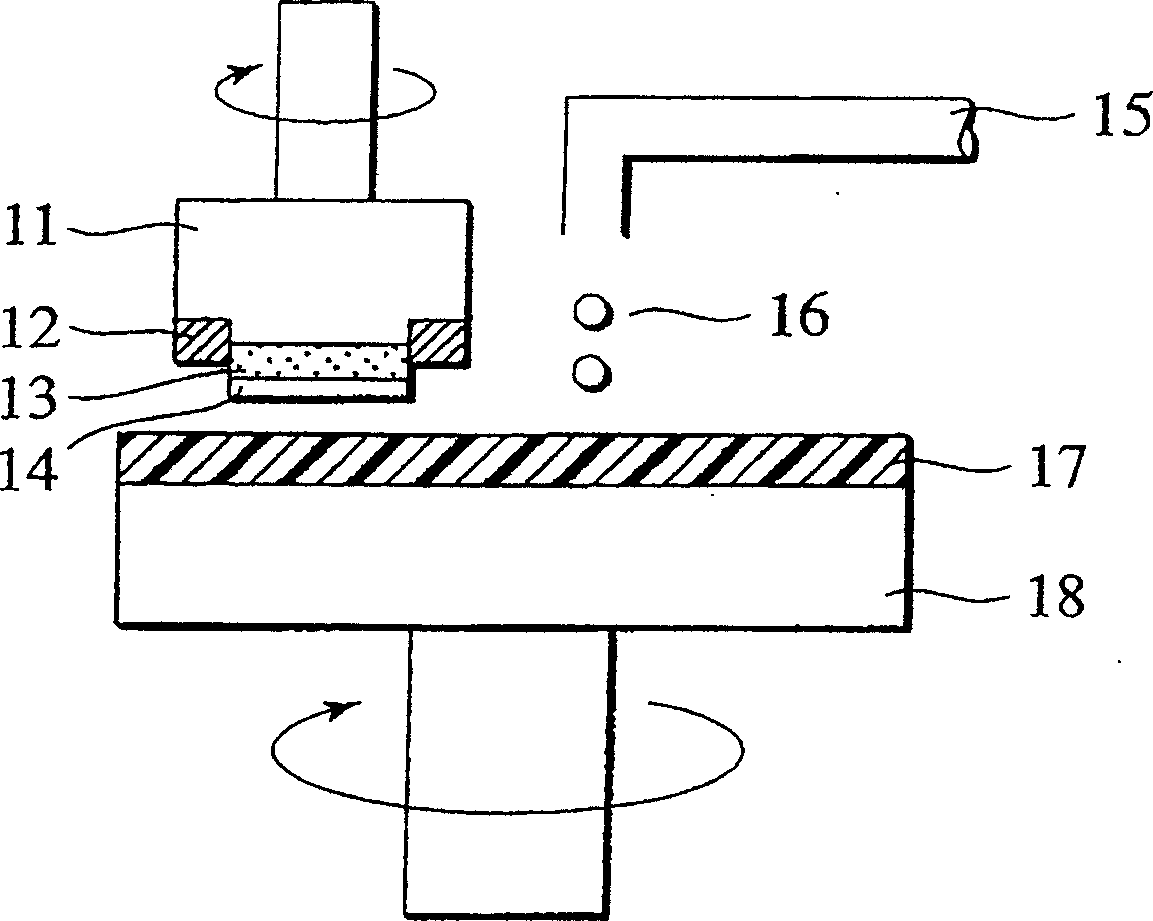
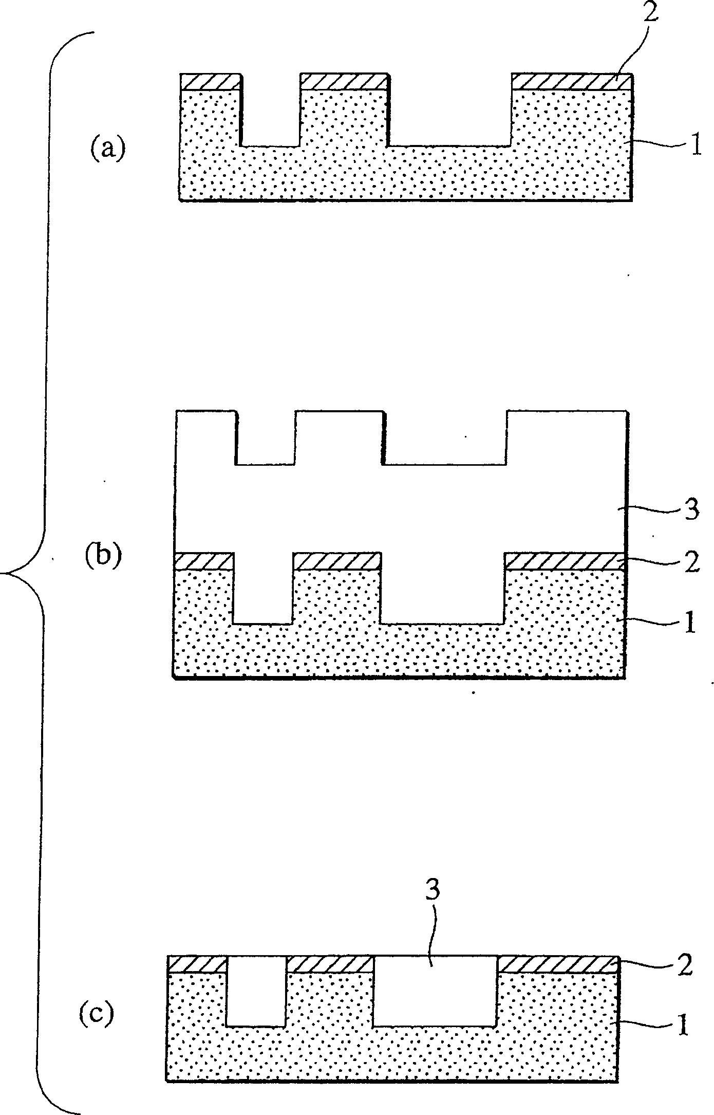
[0128] (Polishing of insulating film layer)
[0129] Using the polishing agent prepared above, the silicon oxide insulating film was polished, dried and washed in the same manner as in Example 2. As a...
PUM
| Property | Measurement | Unit |
|---|---|---|
| density | aaaaa | aaaaa |
| particle size | aaaaa | aaaaa |
| specific surface area | aaaaa | aaaaa |
Abstract
Description
Claims
Application Information