Micro-fluid control chip with surface enhanced Raman spectral active substrate and producing method thereof
A surface-enhanced Raman and microfluidic chip technology, applied in Raman scattering, material excitation analysis, etc., can solve the problem of enhancing the active substrate, etc., and achieve the effect of simple equipment, strong Raman signal, and high activity
- Summary
- Abstract
- Description
- Claims
- Application Information
AI Technical Summary
Problems solved by technology
Method used
Image

Examples
Embodiment 1
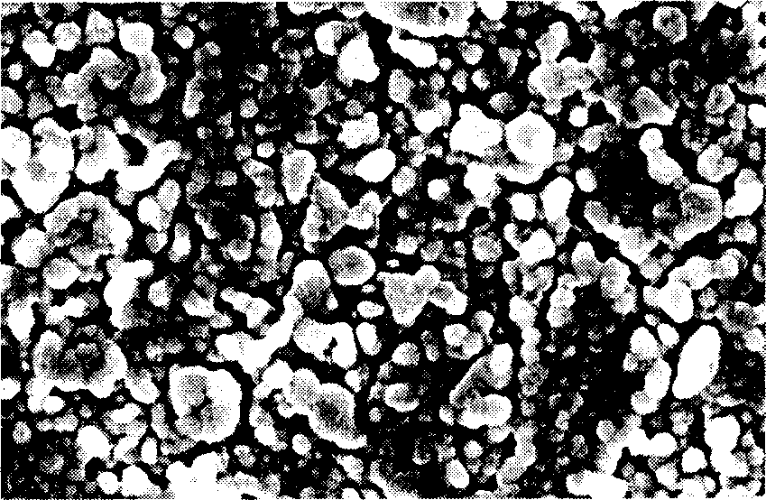
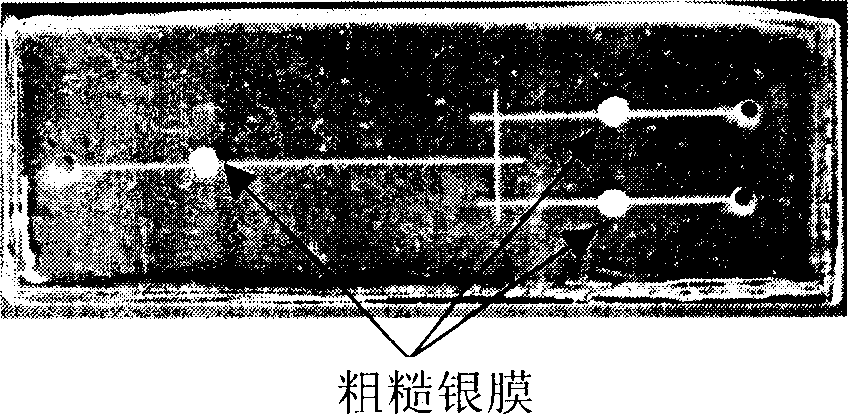
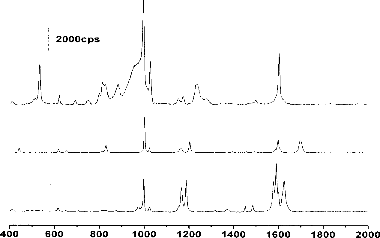
[0025] Stick the PDMS mask sheet with 3 holes (aperture diameter: 2mm) on the standard cleaned glass slide. Using the JS2S-80D sputtering station (produced by Beijing Chuangweina Co., Ltd.), adopting the DC rotary sputtering mode, the titanium film was sputtered with a power of 150W for 7 minutes, and the silver film was sputtered with a power of 160W for 15 minutes. Immerse in 1mol / L KCl solution, and use CHI631B electrochemical workstation (Shanghai Chenhua) to roughen the surface silver film by electrochemical redox (ORC). V, stay at this potential for 10s, slowly return to -0.25V at a rate of 0.01V / s, and fully reduce at -0.25V for 20s until the surface is completely reduced to light yellow fluff. The mask was removed to obtain a glass flake with a partially rough substrate. Three reservoirs were processed on the PDMS coverslip with a puncher; 2 -50F laser marking machine (produced by Beijing Chuangkeyuan Company) to process grooves. Place the cover slip and the glass s...
Embodiment 2
[0028]Attach the PDMS mask sheet with 3 holes (aperture diameter: 2mm) on the freshly peeled PDMS cover slip. Using the DC rotary sputtering mode, the titanium thin film was sputtered with a power of 150W for 7 min, and the gold thin film was sputtered with a power of 150W for 10 min. Immerse in 0.1mol / L KCl solution to roughen the gold film on the surface by ORC. The specific process: first keep the potential at -0.3V, then step to 1.2V at a speed of 1.0V / s, and stay at this potential for 1.5s. Return to -0.3V at a speed of 0.5V / s, and fully restore at -0.3V for 30s. After the above process was cycled 20 times, it was taken out at the potential of -0.3V to obtain a dark brown surface with high SERS activity. The mask was removed to obtain a PDMS substrate with a rough gold base locally. Three reservoirs were processed on the PDMS cover with a puncher; grooves were processed with a laser marking machine. Place the PDMS cover slip and the PDMS substrate with a rough substrat...
Embodiment 3
[0030] Stick the PDMS mask sheet with 3 holes (aperture diameter: 2mm) on the standard cleaned glass slide. The DC rotary sputtering mode was adopted, and the titanium film was sputtered with a power of 150W for 7 minutes, and the copper film was sputtered with a power of 150W for 10 minutes. Immerse in 0.1mol / L KCl solution, step the potential between -0.4V and 0.4V for 5 times, and then take it out at the potential of -0.4V to get a brown SERS active surface. The mask was removed to obtain a glass substrate with a rough copper base locally. Three reservoirs were machined with a laser marking machine on a glass coverslip that was grooved by wet etching. Put the cover sheet and the glass substrate with a rough base into a high-temperature furnace, raise the temperature to 620°C at a rate of 10°C / min, keep it warm for 3.5 hours, and then cool down at a rate of 10°C / min to obtain a piece of Microfluidic chips with surface-enhanced Raman spectroscopy active substrates.
PUM
| Property | Measurement | Unit |
|---|---|---|
| Diameter | aaaaa | aaaaa |
| Diameter | aaaaa | aaaaa |
| Diameter | aaaaa | aaaaa |
Abstract
Description
Claims
Application Information
 - R&D
- Intellectual Property
- Life Sciences
- Materials
- Tech Scout
- Unparalleled Data Quality
- Higher Quality Content
- 60% Fewer Hallucinations
Browse by: Latest US Patents, China's latest patents, Technical Efficacy Thesaurus, Application Domain, Technology Topic, Popular Technical Reports.
© 2025 PatSnap. All rights reserved.Legal|Privacy policy|Modern Slavery Act Transparency Statement|Sitemap|About US| Contact US: help@patsnap.com