Method for reliable contact of probe and nano-electrode of phase transformation memory device unit

A phase-change memory and nano-electrode technology, which is applied in static memory, instruments, and measuring electronics, can solve problems such as inability to perform electrical performance, high contact pressure, and deformation of nano-probes, and achieve reliable contact. The method is practical and convenient , the effect of great practical significance

Active Publication Date: 2006-09-13
SHANGHAI INST OF MICROSYSTEM & INFORMATION TECH CHINESE ACAD OF SCI
View PDF0 Cites 6 Cited by
  • Summary
  • Abstract
  • Description
  • Claims
  • Application Information

AI Technical Summary

Problems solved by technology

These will bring difficulties when using probes to measure the electrical properties of device units in situ
The main problem is the reliable contact between the probe and the electrode. It is difficult to accurately control the good contact between the probe and the electrode in the usual experimental process.
If the contact pressure is too high, the nanometer electrode will be pierced by the probe. In severe cases, the probe will penetrate the phase change material to the bottom electrode, causing a short circuit between the upper and lower electrodes.
On the other hand, if the contact pressure between the probe and the electrode is too large, it will also cause problems such as deformation of the nano-probe and damage to the tip.
In addition, when measuring at low temperature or other conditions, due to the difference in the thermal expansion coefficient of the material, although the contact between the nanoprobe and the electrode material is good at room temperature, there may be problems in the contact between them at low temperature, resulting in Unable to conduct electrical performance test

Method used


Image

  • Method for reliable contact of probe and nano-electrode of phase transformation memory device unit
  • Method for reliable contact of probe and nano-electrode of phase transformation memory device unit
  • Method for reliable contact of probe and nano-electrode of phase transformation memory device unit

Examples


Embodiment 1

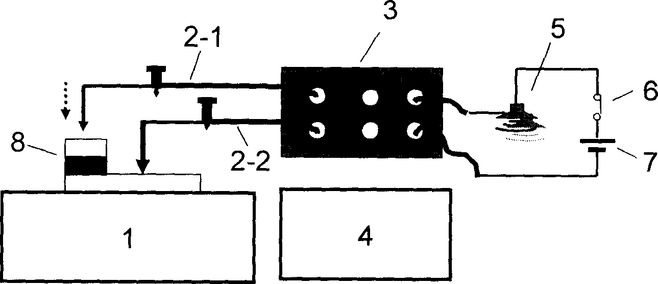
[0038] Embodiment 1: Referring to Fig. 1, the main preparation process and testing method of the sample are as follows:

[0039] (1) The substrate is 500nm thick SiO 2 For the Si sheet of the dielectric film, first use the magnetron sputtering method to grow an 80nm thick Ti / TiN transition layer, and then sputter to prepare a 100nm thick W as the bottom electrode;

[0040] (2) Magnetron sputtering phase change material GeSbTe, the thickness is about 80nm, the background vacuum is 3×10 -6 Torr, the sputtering vacuum is 0.08Pa, and the power is 100W.

[0041] (3) Put the prepared sample on the sample stage shown in Figure 1, adjust the probes, one is in contact with the lower electrode, the other is suspended above the upper electrode, and the two probes are connected to the circuit of the alarm device. Close the switch, slowly adjust the knob, so that the probe above the upper electrode slowly drops, when the alarm alarms, stop adjusting, and turn off the alarm switch.

[00...

Embodiment 2

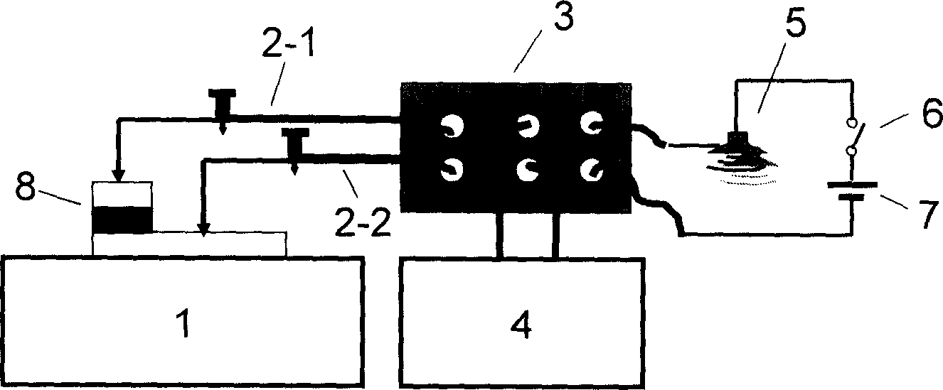
[0044] Embodiment 2: see figure 2 , sample preparation is the same as embodiment one, and the testing method of sample is as follows:

[0045] (1) Open the inflation valve of the vacuum system, fill the sealed chamber with air, open the sealing cover, and put the sample into figure 2 In the cavity shown, adjust the sample stage so that the upper and lower probes are respectively aligned with the upper and lower electrodes of the sample;

[0046] (2) Close the inflatable valve, cover the sealing cover, vacuumize the mechanical pump, adjust the probes, one is in contact with the lower electrode, the other is suspended above the upper electrode, and the two probes are connected to the circuit of the alarm device. Turn on the switch, slowly adjust the knob to make the probe above the upper electrode drop slowly, when the alarm alarms, stop adjusting and turn off the alarm switch.

[0047] (3) Feed liquid nitrogen from the refrigerant inlet, observe the reading of the digital vol...

Embodiment 3

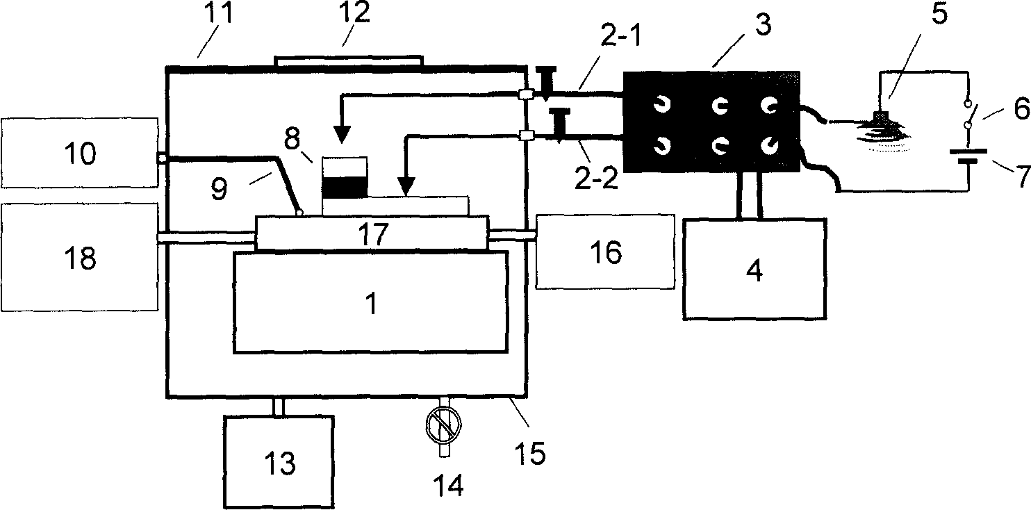
[0050] Embodiment 3: see image 3 , sample preparation is the same as embodiment one, and the testing method of sample is as follows:

[0051] (1) Open the inflation valve of the vacuum system, fill the sealed chamber with air, open the sealing cover, and put the sample into image 3 In the cavity shown, adjust the sample stage so that the upper and lower probes are respectively aligned with the upper and lower electrodes of the sample;

[0052] (2) Close the inflation valve, cover the sealing cover, vacuumize the mechanical pump, adjust the probes, one is in contact with the lower electrode, and the other is suspended above the upper electrode, and the two probes are connected to the circuit of the alarm device. On the switch, adjust the knob slowly to make the probe above the upper electrode drop slowly. When the alarm alarms, stop adjusting and turn off the alarm switch;

[0053] (3) Heat the hot plate through the heating control system, and observe the reading of the dig...


PUM


Abstract

A method for realizing reliable contact of probe to nanoelectrode of phase transformation storage includes series ¿C connecting test probe and sample to be tested in a peripheral DC circuit, regulating lift knob slowly and carefully, connecting peripheral DC circuit through and making alarm by alarm series ¿C connected in DC loop when probe pointer is contacted with surface of sample so as ,to present that probe pointer is contacted with sample for enabling to carry out electrical property measurement of sample. The said method can protect sample effectively for avoiding nano-electrode and phase transformation material to be damaged by probe pointer.

Description

technical field [0001] The invention relates to a method for realizing reliable contact between a probe and a nano-electrode of a phase-change memory device unit, more precisely, it relates to a method for measuring the nano-electrode and the electrical measurement method of an anti-irradiation phase-change memory device unit and other electronic devices. The reliable contact and positioning control of a probe is a simple and practical method for measuring a nanometer electrode device unit, and belongs to the field of preparation technology and electrical characterization of nanomaterials in microelectronics. Background technique [0002] With the continuous reduction of semiconductor devices and the higher and higher requirements for storage capacity, existing memories face many challenges, such as the large power consumption caused by the leakage current of dynamic random access memory (DRAM), static random access The area occupied by the memory (SRAM) is too large, and th...

Claims


Application Information

Patent Timeline
Patent Type & Authority Applications(China)
IPC IPC(8): G11C29/00G01R31/00
Inventor 宋志棠吴良才刘波封松林
Owner SHANGHAI INST OF MICROSYSTEM & INFORMATION TECH CHINESE ACAD OF SCI
Why Eureka
Try Eureka