

LCD disply device and manufacture thereof
A liquid crystal display device and transistor technology, which can be used in identification devices, semiconductor/solid-state device manufacturing, photolithographic process exposure devices, etc., and can solve problems such as unsatisfactory standards and affecting exposure.
- Summary
- Abstract
- Description
- Claims
- Application Information
AI Technical Summary
Problems solved by technology
Method used
Image

Examples
Embodiment 1
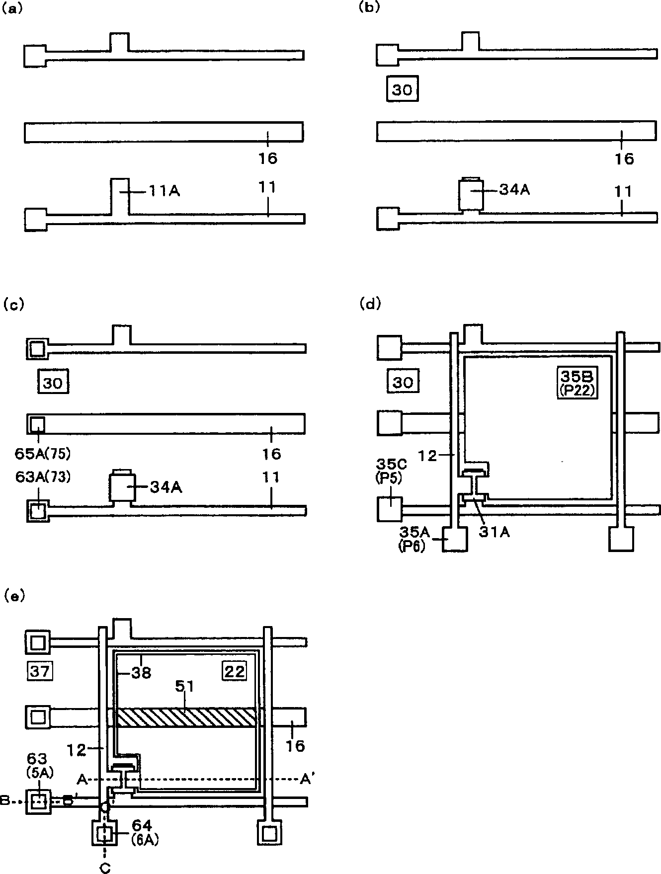
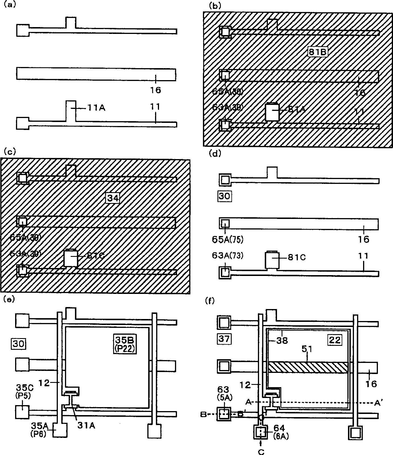
[0179] According to Embodiment 1, first, on one main plane of the glass substrate 2, use a vacuum film-forming device such as SPT to coat the first metal layer with a film thickness of about 0.1-0.3 μm, such as heat-resistant metals such as Cr, Ta, Mo or It is an alloy or silicide of the above substances. If necessary, AL or AL alloy may be used and laminated with a related metal substance having high heat resistance in order to achieve low resistance. Next, if figure 1 (A) with figure 2 As shown in (A), the scanning line 11 and the accumulation capacitance line 16 which also serve as the gate 11A are selectively formed by microfabrication technology. In addition, when the accumulation capacitance 15 is formed between the pixel electrode (drain) and the preceding scanning line, the accumulation capacitance line 16 is not an essential component.
[0180] Next, a PCVD device is used on the whole glass substrate 2, for example, the first SiNx layer 30 composed of a gate insu...
Embodiment 2
[0190] Embodiment 2 is the same as Embodiment 1. First, on one main plane of the glass substrate 2, use a vacuum film-forming device such as SPT to coat the first metal layer with a film thickness of about 0.1-0.3 μm, such as Cr, Ta, Mo, etc. Refractory metals or alloys or silicides of the above substances, such as image 3 (A) with Figure 4 As shown in (A), the scanning line 11 and the accumulation capacitance line 16 which also serve as the gate 11A are selectively formed.
[0191] The second is to use a PCVD device on the whole glass substrate 2, for example, the first SiNx layer 30, which is composed of a gate insulating layer with a film thickness of about 0.3-0.2-0.05 μm, and contains almost no impurities. The first amorphous silicon layer 31 composed of the channel, and the second amorphous silicon layer 33 composed of the source / drain of the insulated gate transistor and three thin film layers containing impurities such as phosphorus, continue to use Vacuum film-for...
Embodiment 3
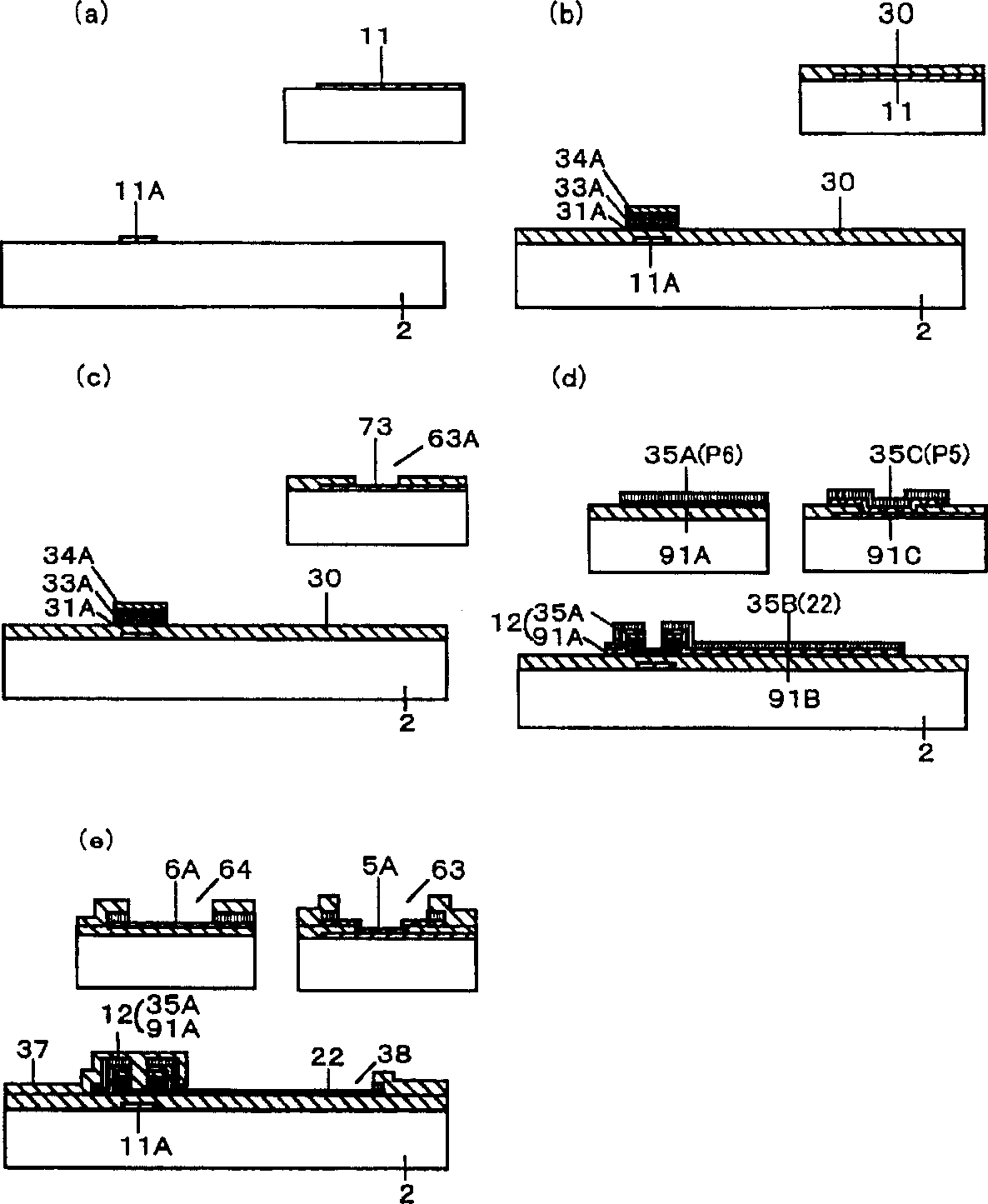
[0204] In Embodiment 3, after the scanning lines 11 and the accumulation capacitance lines 16 are formed, the first amorphous silicon layer 31 and the insulating gate containing impurities such as phosphorous are sequentially covered, for example, with a film thickness of about 0.3-0.2-0.05 μm. After the second amorphous silicon layer 33 and three kinds of thin film layers composed of the source / drain electrodes of the type transistor, continue to use a vacuum film forming device such as SPT to coat a heat-resistant metal layer with a film thickness of about 0.1 μm, such as Ti , Cr, Mo and other heat-resistant metals or the thin film layer 34 composed of silicides of the above-mentioned substances, all are carried out according to the same process as in Example 1.
[0205] Such as Figure 5 (B) with Figure 6 As shown in (B), after microfabrication technology, the heat-resistant metal layer 34, the second amorphous silicon layer 33, and the first amorphous silicon layer 31 ar...
PUM
| Property | Measurement | Unit |
|---|---|---|
| Thickness | aaaaa | aaaaa |
| Thickness | aaaaa | aaaaa |
| Thickness | aaaaa | aaaaa |
Abstract
Description
Claims
Application Information