Non-volatile memory component based on RbAg4I5 film and producing method thereof

A memory element, non-volatile technology, applied in the field of non-volatile phase change memory element and its preparation, can solve the problems of not being used in large quantities, large energy consumption, inability to achieve fast reading and writing, etc.

Inactive Publication Date: 2007-01-03
NANJING UNIV
View PDF0 Cites 5 Cited by
  • Summary
  • Abstract
  • Description
  • Claims
  • Application Information

AI Technical Summary

Problems solved by technology

The former mainly includes dynamic random access memory (DRAM), which has the advantages of fast reading and writing, but the outside world must provide uninterrupted power supply during work, so there is a large energy consumption during work, and the stored information disappears immediately when the power is cut off
The latter is mainly magnetic media storage, because the magnetic head and the recording medium have to move mechanically during the reading and writing process, so fast reading and writing cannot be achieved.
In addition, there are ferroelectric memory (FeRAM) under research, M-RAM based on spintronic materials, etc., which have not yet been widely used due to some of their weaknesses

Method used


Image

  • Non-volatile memory component based on RbAg4I5 film and producing method thereof
  • Non-volatile memory component based on RbAg4I5 film and producing method thereof
  • Non-volatile memory component based on RbAg4I5 film and producing method thereof

Examples


Embodiment 1

[0060] Embodiment 1. Based on solid electrolyte RbAg 4 I 5 The preparation method of the non-volatile phase-change memory element, its preparation steps are as follows:

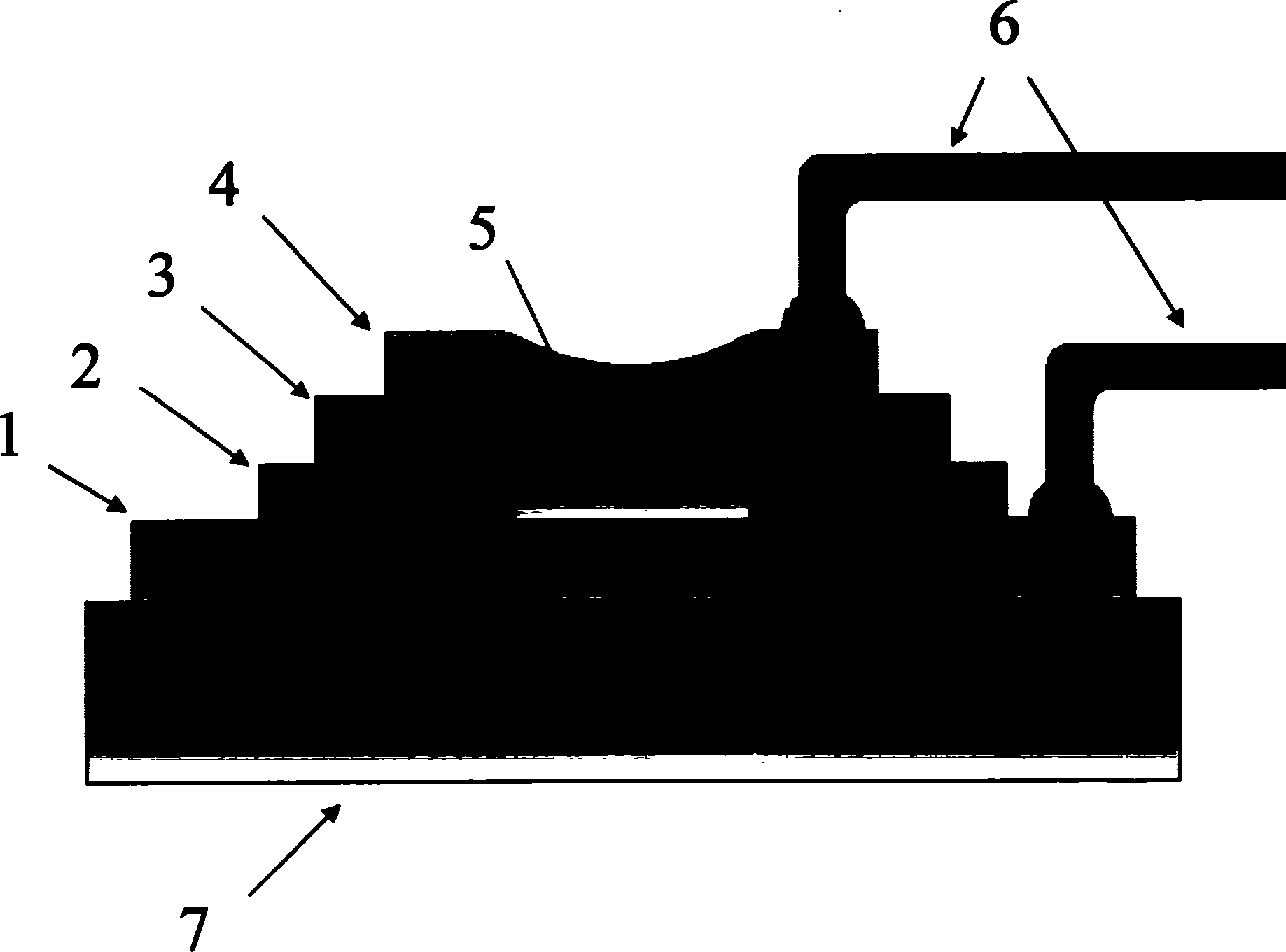
[0061] (1), deposit non-reactive electrode film 1 with pulse laser deposition method on silicon chip substrate 7, its material is platinum, and the thickness of non-reactive electrode film 1 is 200 nanometers;

[0062] (2), utilize radio frequency magnetron sputtering method to deposit one deck insulating layer 2 on non-reactive electrode film 1, the material of insulating layer is silicon dioxide, and its thickness is 100 nanometers;

[0063] (3), in the insulating layer 2, utilize the focused particle beam etching method to process a micropore 5 with a diameter of 200 nanometers, exposing the non-reactive electrode film 1 at the bottom;

[0064] (4) Cover the substrate with the microholes 5 with a metal mask that is engraved with a hole with a diameter of 0.5 mm, and align the holes of the mask with the h...

Embodiment 2

[0069] Embodiment 2. Based on solid electrolyte RbAg 4 I 5 The non-volatile phase change memory element and the preparation method, the specific preparation steps are as follows:.

[0070] (1), deposit non-reactive electrode film 1 with magnetron sputtering method on quartz glass plate substrate 7, its material is gold, and the thickness of non-reactive electrode film 1 is 1 micron;

[0071] (2), utilize radio frequency magnetron sputtering method to deposit one deck insulating layer 2 on non-reactive electrode film 1, the material of insulating layer is silicon dioxide, and its thickness is 200 nanometers, uses silicon dioxide ceramic target during sputtering, Argon with a pressure of 10Pa is used as the sputtering gas, and the minimum temperature of the lining is 80°C;

[0072] (3), utilize the electron beam etching method to process the micropore 5 that diameter is 10 microns in insulating layer 2, expose the gold non-reactive electrode film 1 of bottom;

[0073] (4), co...

Embodiment 3

[0078] Embodiment 3. is used to prepare the solid electrolyte RbAg of non-volatile phase-change memory element 4 I 5 The preparation method of film material, its preparation steps are as follows:

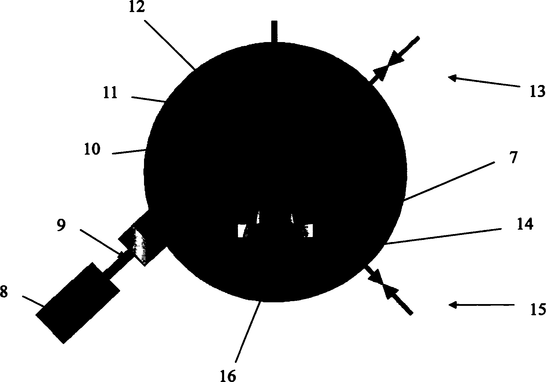
[0079] (1) RbAg 4 I 5 The single-phase ceramic target (10) is made of RbAg 4 I 5 Prepared by powder sintering: melting a mixture of 80mol% AgI and 20mol% RbI at 400°C, quenching the mixture to room temperature with water, grinding the obtained block into powder and heat treatment at 150°C for 14h, then RbAg 4 I 5 The powder is statically pressed at room temperature under 14MPa into a Φ21×4mm disc, and the disc is sintered at 150°C for 8 hours in a box-type electric furnace;

[0080] (2) RbAg 4 I 5 The single-phase ceramic target (10) is fixed on the target table (11) of the pulse laser deposition film forming system, the substrate (7) is fixed on the substrate table (14), and the resistance heating furnace (16) is arranged on the substrate table ( 14), they are all placed i...


PUM

PropertyMeasurementUnit
thicknessaaaaaaaaaa
wavelengthaaaaaaaaaa
energyaaaaaaaaaa

Abstract

The present invention discloses resistance switch effect based non-volatilisation phase transition memory element physical design preparation method. It contains setting solid electrolyte RbAg 4I5 film between reaction electrode and non - reaction electrode to construct one miniature sandwich structure of memory unit, said memory unit together with substrate and insulating layer all having five layers, depositing single-layer non - reaction electrode on substrate, depositing single-layer insulating layer on non - reaction electrode, and etching one micro pore in it to expose non - reaction electrode, depositing single-layer RbAg 4I5 film on insulating layer, thereon depositing single-layer reaction electrode, respectively leading out leading wire on non - reaction electrode and reaction electrode. Said memory element has advantages of compactness, simple structure, non-volatilisation, rapid read-write, low operating voltage and energy consumption, non - moving part, and nondestructive readout etc.

Description

1. Technical field [0001] The invention belongs to the field of microelectronic devices and materials thereof, and in particular relates to a novel high-density solid-electrolyte RbAg-based solid electrolyte that can be quickly read and written and applied to integrated circuits. 4 I 5 A non-volatile phase-change memory element and a preparation method thereof. 2. Background technology [0002] For nearly half a century, the development of integrated circuits has basically followed the prediction made by G.E. Moore: "The number of components integrated on a single chip doubles every eighteen months", that is, Moore's Law. When the size of silicon-based CMOS devices is gradually reduced to the nanometer level, traditional devices are getting closer and closer to the limits of physics and technology. In order to follow the development trend of integrated circuit technology, the construction of new semiconductor devices must rely on new devices with simple structures and easi...

Claims


Application Information

Patent Timeline
Patent Type & Authority Applications(China)
IPC IPC(8): H01L45/00C23C14/22G11C11/56
Inventor 刘治国梁雪飞陈涌
Owner NANJING UNIV
Why Eureka
Try Eureka