
MEMS micro high sensitivity magnetic field sensor and manufacturing method
A magnetic field sensor, high-sensitivity technology, applied in the size/direction of the magnetic field, the use of magneto-optical equipment for magnetic field measurement, instruments, etc.
- Summary
- Abstract
- Description
- Claims
- Application Information
AI Technical Summary
Problems solved by technology
Method used
Image

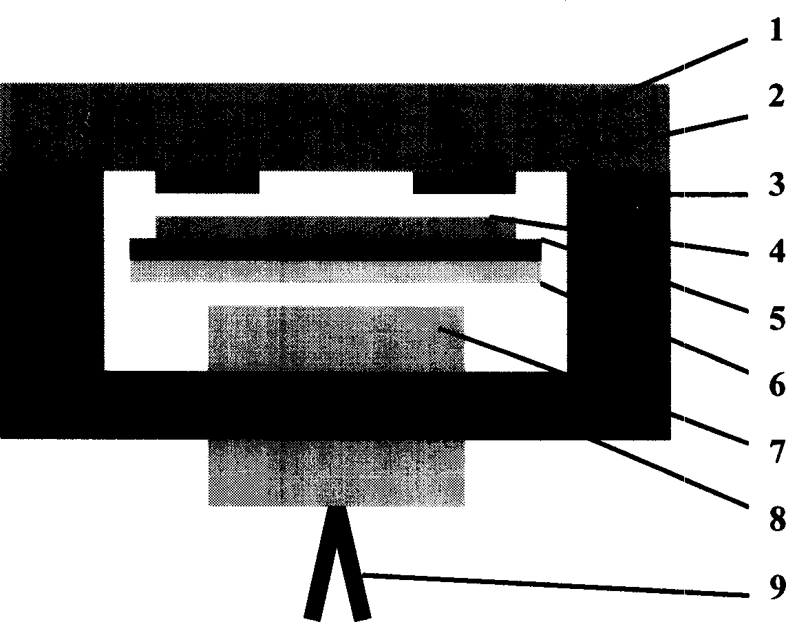
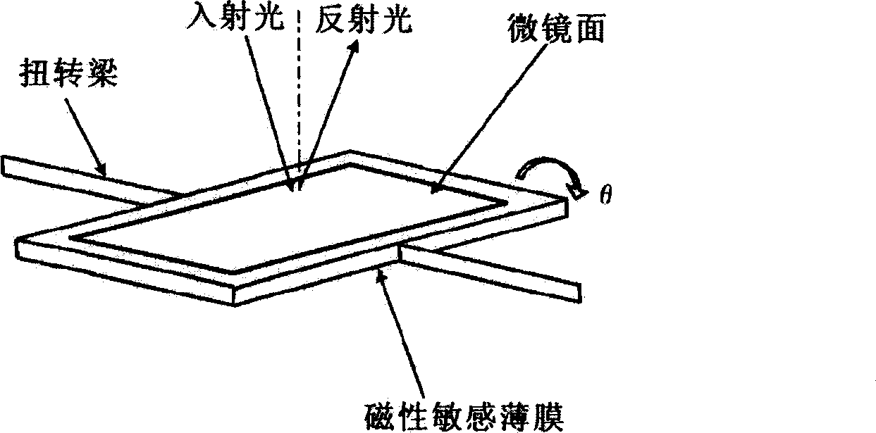
Examples
Embodiment
[0098] Embodiment: The specific process implementation method of MEMS high-sensitivity magnetic field sensor is as follows:
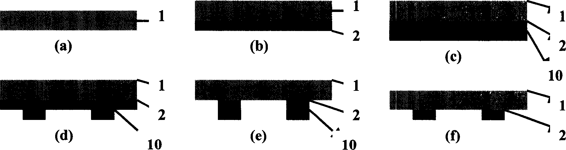
[0099] (1) First, on the Pyrex7740 glass support body 1, the metal aluminum electrode material 2 is evaporated by sputtering or electron beam, such as image 3 (b) shown.
[0100] (2) Select semiconductor materials such as silicon wafer 1 (ordinary P+ type (100) double throw silicon wafer ( Figure 4 a), the thickness is 420±20 microns, the resistivity is 0.01-0.02 ohm cm), and the glue is applied ( image 3 c), photolithography development ( image 3 d) After that, by corrosion ( image 3 e), to glue ( image 3 f) and other processes to realize the patterned production of the feedback electrode 2 .
[0101] (3) By etching on the substrate silicon, SOI or other materials ( Figure 4 a) Upper glue ( Figure 4 b), photolithography and development to get as Figure 4 (c) The patterned mask shown.
PUM
| Property | Measurement | Unit |
|---|---|---|
| thickness | aaaaa | aaaaa |
| thickness | aaaaa | aaaaa |
| Sensitivity | aaaaa | aaaaa |
Abstract
Description
Claims
Application Information