Method for realizing nitride semiconductor device inter-active-area isolation utilizing boron ion injection

A technology of nitride semiconductors and boron ions, which is applied in semiconductor/solid-state device manufacturing, electrical components, circuits, etc., can solve problems affecting interconnection connection and device yield, so as to save production steps, improve performance and finished products rate, lowering the height effect

Inactive Publication Date: 2007-03-28
NO 55 INST CHINA ELECTRONIC SCI & TECHNOLOGYGROUP CO LTD
View PDF0 Cites 8 Cited by
  • Summary
  • Abstract
  • Description
  • Claims
  • Application Information

AI Technical Summary

Problems solved by technology

[0004] The purpose of the present invention is to solve the problem that the height of the mesa affects the connection of the interconnection line and the yield of the device in the mesa electrical isolation method used in the existing nitride semiconductor device...

Method used


Image

  • Method for realizing nitride semiconductor device inter-active-area isolation utilizing boron ion injection
  • Method for realizing nitride semiconductor device inter-active-area isolation utilizing boron ion injection
  • Method for realizing nitride semiconductor device inter-active-area isolation utilizing boron ion injection

Examples


Embodiment 1

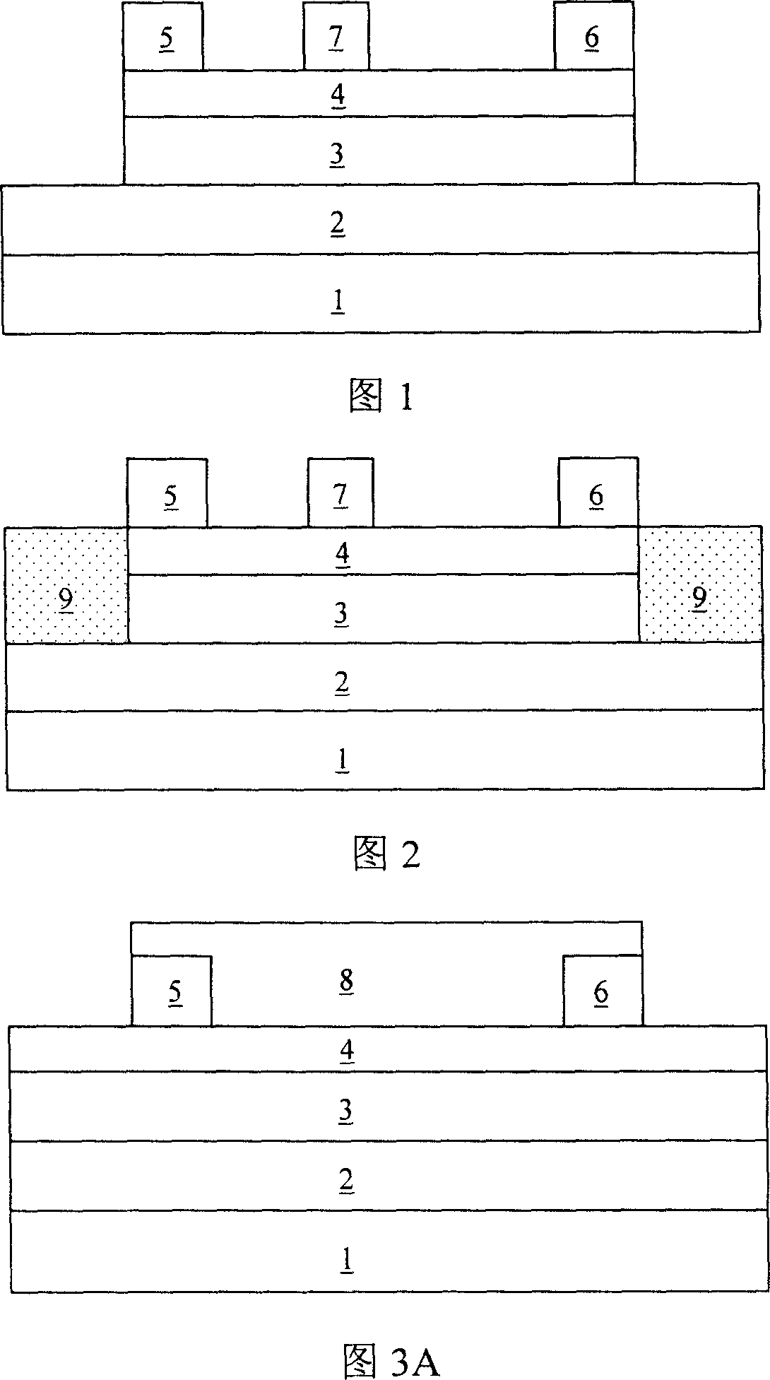
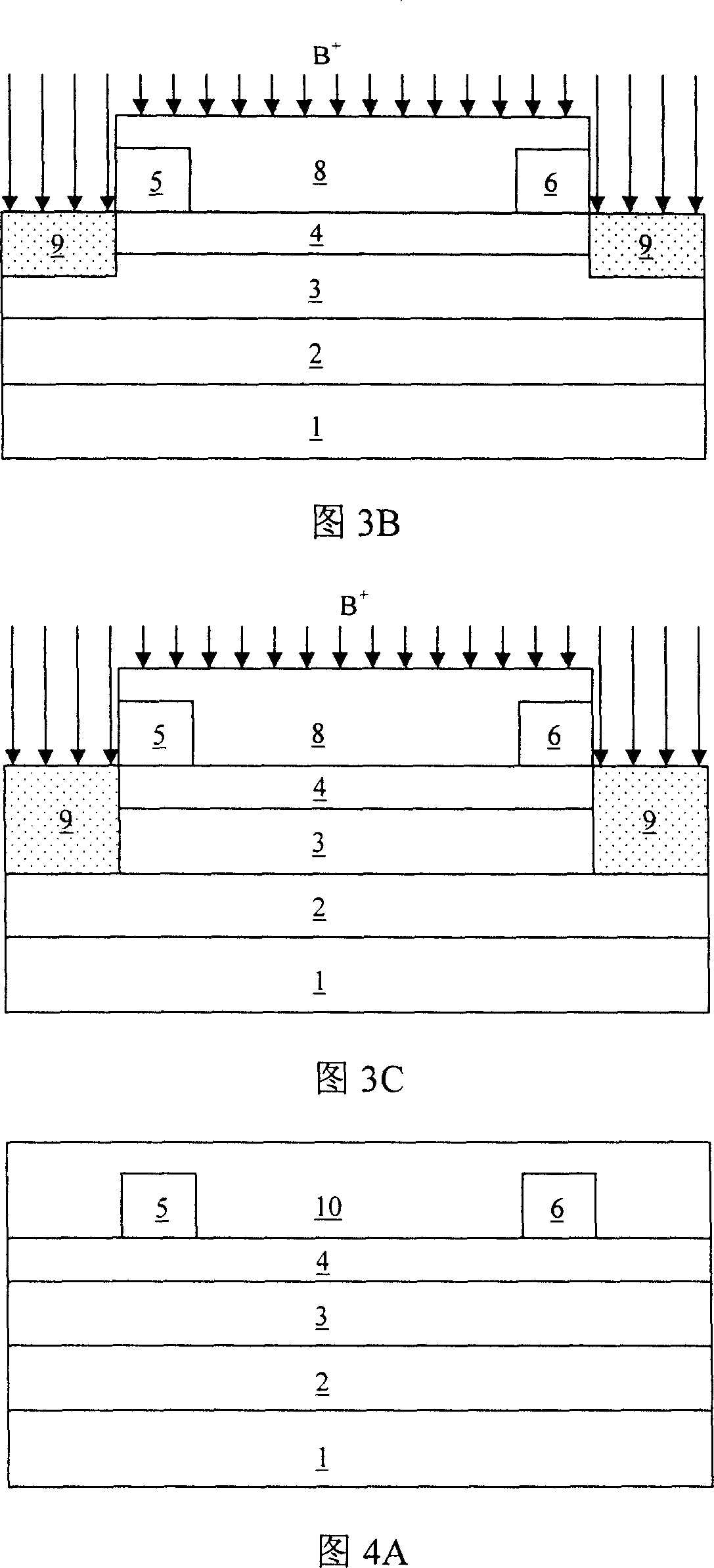
[0027] As shown in Figure 2, 3A-3C, 5.

[0028] The AlGaN / GaN heterojunction material in Fig. 2 includes substrate 1, buffer layer 2, channel layer 3 and barrier layer 4, channel layer 3 and barrier layer 4 between devices, between AlGaN / GaN HEMT The intervening channel layer 3 and barrier layer 4 are bombarded by high-energy ion beams to form a high-resistance damaged layer 9, which realizes electrical isolation between devices. The specific production process is:

[0029] As shown in Figure 3A, the first ohmic contact region 5 is formed on the barrier layer 4 of the AlGaN / GaN heterojunction material as the source electrode, and then the barrier layer 4 is separated from the first ohmic contact region by 2 micrometers to 5 micrometers. The method of forming the second ohmic contact region 6 as the drain electrode and forming the ohmic contact with the AlGaN barrier layer is well known in the art and will not be repeated here. A mask 8 is used to protect the AlGaN / GaN hetero...

Embodiment 2

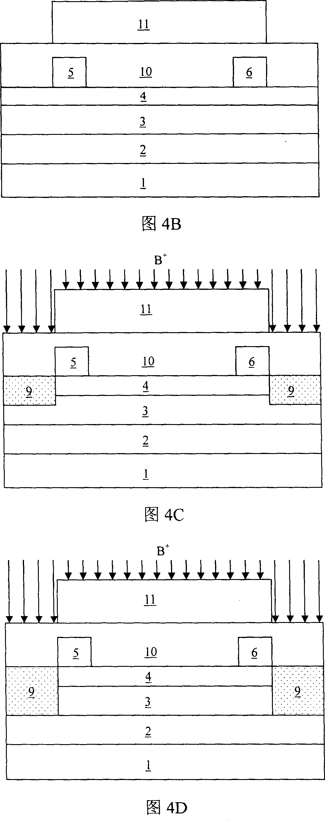
[0035] As shown in Figures 2, 4A-4D.

[0036] As shown in FIG. 4A, a source ohmic contact 5 and a drain ohmic contact 6 are formed on the AlGaN / GaN heterojunction as in Example 1, and a dielectric layer 10 is deposited on the exposed surface of the barrier layer 4, the source electrode 5 and the drain electrode. On pole 6, optional materials for the dielectric layer include but are not limited to silicon nitride (SiN), silicon oxide (SiO 2 ), aluminum nitride (AlN), aluminum oxide (Al 2 o 3 ), the dielectric layer deposition methods include but not limited to sputtering, electron beam evaporation, plasma enhanced chemical vapor deposition (PECVD), and the thickness of the dielectric layer is about 100nm. As shown in FIG. 4B , a mask 11 is used to protect the AlGaN / GaN heterojunction material and parts of the device that do not require ion implantation, and the preferred material of the mask 11 is photoresist.

[0037] As shown in Figure 4C, boron ions with an implantation e...


PUM

PropertyMeasurementUnit
Thicknessaaaaaaaaaa
Thicknessaaaaaaaaaa

Abstract

Aiming at issues of influencing on connection of interconnection line caused by height of tabletop and low yield existed in insulation of tabletop adopted by nitride semiconductor device, the invention discloses method of electrics insulation between active areas of nitride semiconductor device by using boron ion implantation. The method includes steps: after forming source ohmic contact and drain ohmic contact on AlGaN/GaN hetero junction, the method protects place, where ion implantation is not needed to carry out, of surface of AlGaN/GaN hetero junction material and device by using mask; forming high resistance damage zone on the said place not protected by using boron ion bombardment one or two times. Ensuring electrics insulation for device, the invention raises performance of device and is in favor of raising yield.

Description

technical field [0001] The invention relates to a semiconductor manufacturing technology, in particular to an isolation method for improving the isolation effect between active regions of nitride semiconductors and the yield of products, in particular to a method for realizing nitride semiconductor devices by boron ion implantation method of isolation between the active regions. Background technique [0002] Devices based on gallium nitride (GaN) are the current research focus of compound semiconductor devices and circuits. In the fabrication of aluminum gallium nitride (AlGaN) / gallium nitride high electron mobility transistors (HEMT) and their circuits, in order to make the device Electrical isolation between the active regions of the device is required for proper operation of the circuit. The most commonly used isolation method is mesa isolation, which achieves electrical isolation between devices by removing the active layer between devices. Figure 1 shows a general sche...

Claims


Application Information

Patent Timeline
IPC IPC(8): H01L21/82H01L21/76
Inventor 陈堂胜焦刚李肖任春江
Owner NO 55 INST CHINA ELECTRONIC SCI & TECHNOLOGYGROUP CO LTD
Why Eureka
Try Eureka