Aluminium gallium nitride/gallium nitride high electronic migration rate transistor and its manufacturing method

A high electron mobility, aluminum gallium nitride technology, used in semiconductor/solid-state device manufacturing, circuits, electrical components, etc., can solve problems affecting device frequency characteristics, etc. Effect of gate leakage current

Inactive Publication Date: 2007-03-28
NO 55 INST CHINA ELECTRONIC SCI & TECHNOLOGYGROUP CO LTD
View PDF0 Cites 15 Cited by
  • Summary
  • Abstract
  • Description
  • Claims
  • Application Information

AI Technical Summary

Problems solved by technology

[0010] The introduction of a dielectric layer 51 with a high breakdown electric field strength between the metal gate 8 and the barrier layer 4 in the device 1 reduces the leakage current on the metal gate 8 and correspondingly increa

Method used


Image

  • Aluminium gallium nitride/gallium nitride high electronic migration rate transistor and its manufacturing method
  • Aluminium gallium nitride/gallium nitride high electronic migration rate transistor and its manufacturing method
  • Aluminium gallium nitride/gallium nitride high electronic migration rate transistor and its manufacturing method

Examples


Embodiment 1

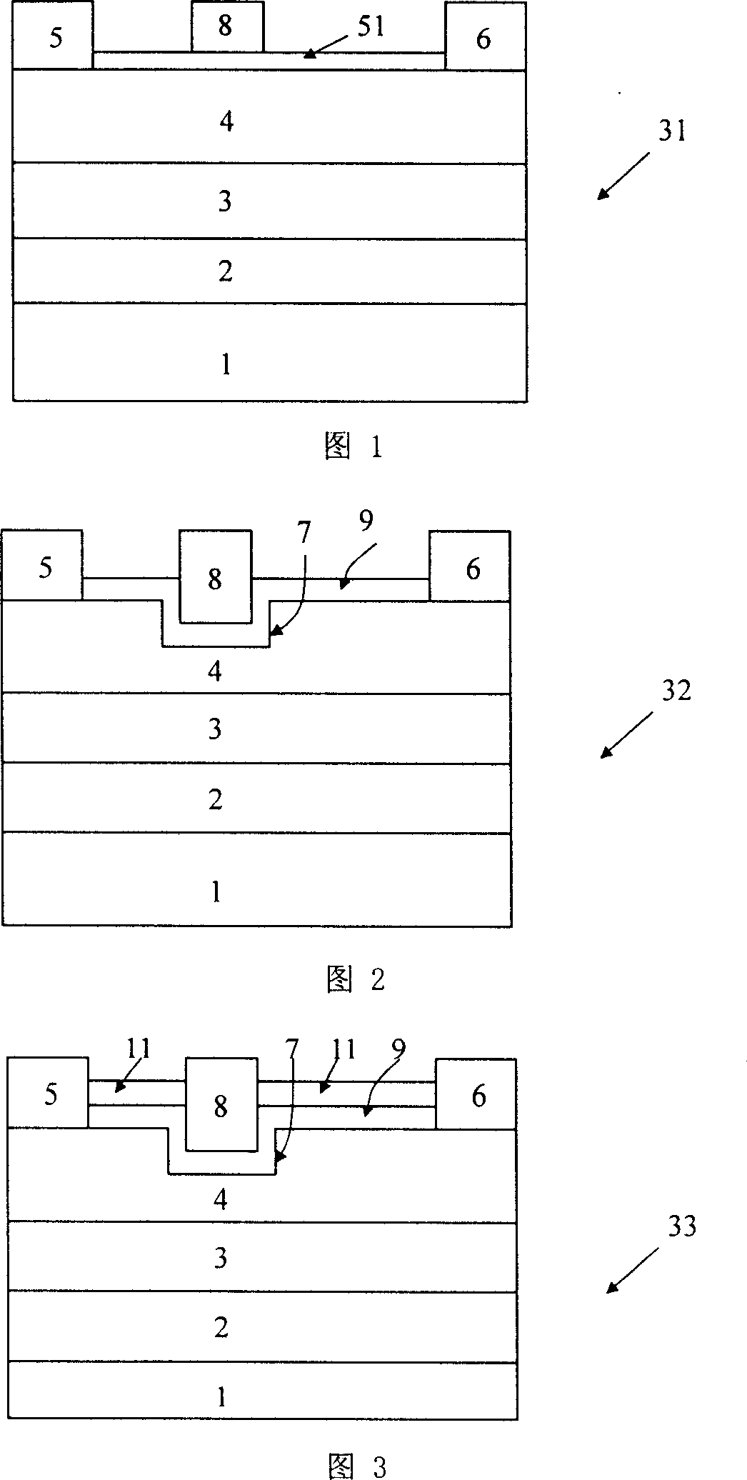
[0061] Figure 2 shows a device 32 of an embodiment of the invention. In the device 32, 1 is a substrate, 2 is a buffer layer, 3 is a GaN channel layer, and 4 is an Al X Ga 1-x N (018 cm -3 . The buffer layer 2, the channel layer 3, and the barrier layer 4 are obtained by epitaxial growth on the substrate 1 sequentially by MOCVD, RF-MBE or any other suitable growth method, and the specific growth process can refer to relevant literature.

[0062] On the barrier layer provide ohmic contact electrode 5 as source electrode, ohmic contact electrode 6 as drain electrode, source electrode 5 and drain electrode 6 can be Ti / Al / Ni / Au, Ti / Al / Mo / Au, Ti / Al / Ti / Au or any other suitable material that can form an ohmic contact with the barrier layer, the metal on the source electrode 5 and the drain electrode 6 is preferably formed by electron beam evaporation, and rapidly annealed at a high temperature of 780°C to 900°C for 30s or so, nitrogen gas is needed during the rapid annealing pro...

Embodiment 2

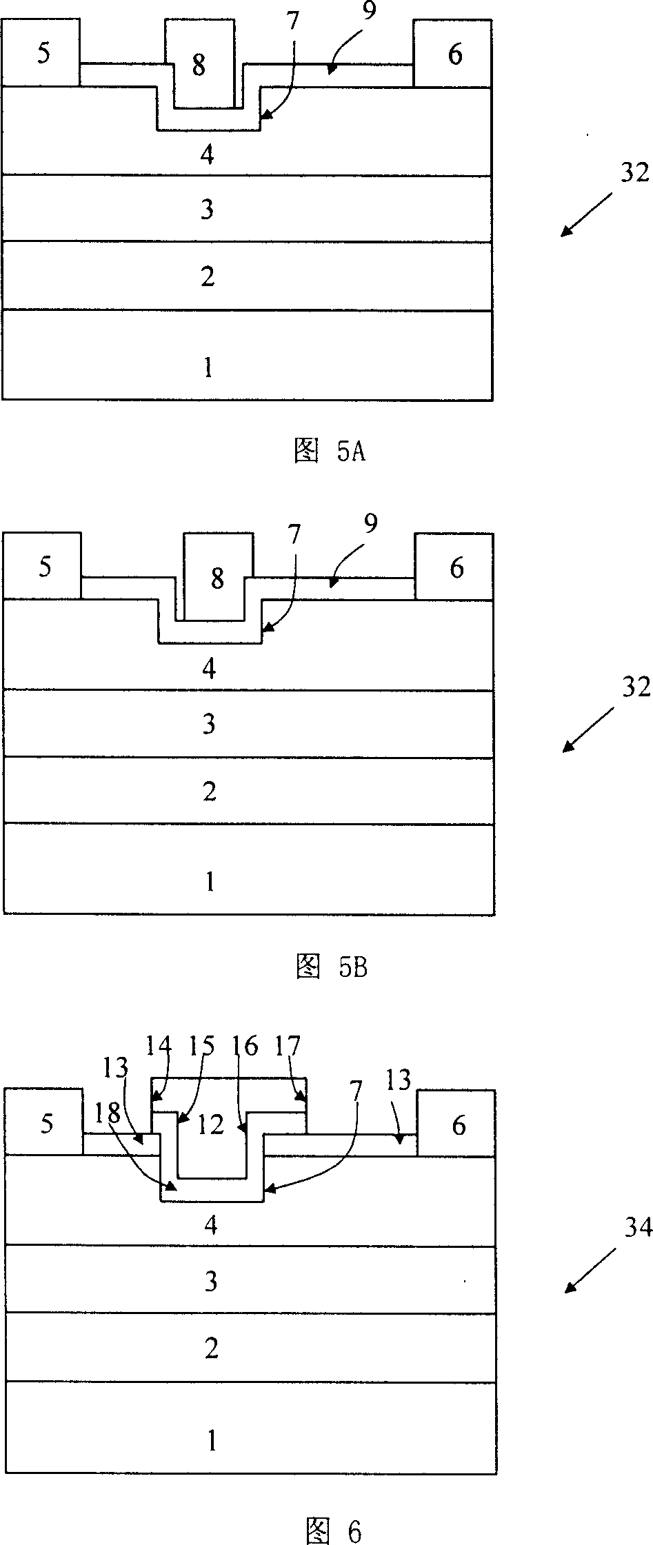
[0079] FIG. 6 is a device 34 with a "T" gate according to one embodiment of the present invention. Similar to device 32 in FIG. 2 , device 34 has substrate 1 , buffer layer 2 , GaN channel layer 3 and AlGaN barrier layer 4 . The device 34 also has a source electrode 5 and a drain electrode 6 located on the barrier layer with the device 32. The surface of the device 34 is covered by the dielectric layer 13 except for the groove 7, and the bottom and side walls of the groove are covered by the dielectric layer 18. The dielectric layer 18 extends toward the source electrode 5 and the drain electrode 6 on the surface of the device and covers the dielectric layer 13. The dielectric layer 18 exists only under the gate electrode 12, and the gate electrode 12 of the device is a "T" gate structure. The distance between sidewalls 14 and 15 in the "T"-shaped grid 12 is less than 0.5 micron, and the distance between sidewalls 16 and 17 is about 1 micron, that is, the "T"-shaped grid 12 is...

Embodiment 3

[0096] FIG. 8 shows a device 36 with a "T" gate according to another embodiment of the present invention. Same as the device in the previous embodiment, the device 36 has a substrate 1, a buffer layer 2, a GaN channel layer 3, an AlGaN barrier layer 4, a source electrode 5 and a drain electrode 6 on the barrier layer, and the surface of the device 36 except The outside of the groove 7 is covered by a dielectric layer 13, and the dielectric layer 18 not only exists under the gate metal but also covers the exposed part of the dielectric layer 13. The gate electrode 12 of the device 36 is the same as the device 34. It has a "T" gate structure . Similarly, the distance between the sidewalls 14 and 15 is less than 0.5 micron, and the distance between the sidewalls 16 and 17 is about 1 micron, so as to improve the performance of the AlGaN / GaN HEMT.

[0097] The formation of the buffer layer 2, the GaN channel layer 3, the AlGaN barrier layer 4, the source electrode 5 and the drain ...


PUM

PropertyMeasurementUnit
Thicknessaaaaaaaaaa
Thicknessaaaaaaaaaa

Abstract

Duplex conflicts exist in current semiconductor device: high breakdown voltage but small transconductance; or large transconductance but low breakdown voltage. The disclosed high electron mobility transistor of nitride of aluminum gallium/ gallium nitride possesses advantages of both. The invention also discloses preparation method. The method includes steps and structures: the disclosed transistor includes channel layer, barrier layer as well as source pole and drain pole setup on the barrier layer; providing groove on the barrier layer between source pole and drain pole; quadrate or T type gate electrode is installed on groove covered by dielectric layer; function of dielectric layer is to reduce leakage current on gate electrode, and increase maximum current of device; function of groove is to raise transconductance of device. Advantages are: retaining large transconductance, small leakage current of gate electrode, and large drive current.

Description

technical field [0001] The invention relates to a semiconductor structure and a manufacturing method thereof, in particular to an aluminum gallium nitride / gallium nitride high electron mobility transistor and a manufacturing method thereof. Background technique [0002] At present, the use of semiconductor solid-state devices in microwave systems can effectively reduce the size of the system and improve reliability. With the development of science and technology, various microwave application systems urgently need electronic devices suitable for high temperature, high frequency, high power, and radiation resistance. All aspects are greatly restricted, so it is necessary to find new semiconductor materials to replace Si and GaAs. GaN is a new type of wide-bandgap semiconductor material. The insulated gate aluminum gallium nitride (AlGaN) / gallium nitride (GaN) HEMT based on it has comparable output power density, high temperature resistance and radiation resistance compared w...

Claims


Application Information

Patent Timeline
IPC IPC(8): H01L29/78H01L29/423H01L21/336H01L21/28
Inventor 陈堂胜焦刚任春江陈辰
Owner NO 55 INST CHINA ELECTRONIC SCI & TECHNOLOGYGROUP CO LTD
Why Eureka
Try Eureka