

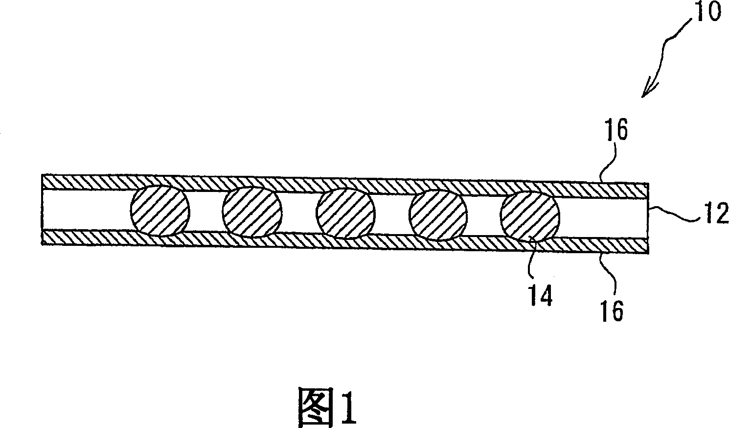
Anisotropic conductive film and manufacturing method thereof
An anisotropic and manufacturing method technology, applied in cable/conductor manufacturing, conductive connection, conductive adhesive and other directions, can solve the problems of lack of mass production of long objects, increased manufacturing cost, no disclosure, etc., and achieve easy mass production. The effect of production, cheap manufacturing, simple and manufactured
- Summary
- Abstract
- Description
- Claims
- Application Information
AI Technical Summary
Problems solved by technology
Method used
Image

Examples
Embodiment 1
[0142] To a solution of polysulfone (manufactured by Aldrichichi, molecular weight Mw=56,000) dissolved in chloroform at a concentration of 0.1 [wt%], 10 [wt%] of dodecyl acrylamide and hexanoic acid were added to the polysulfone. As an amphiphilic substance, the copolymer is formulated into a polymer solution.
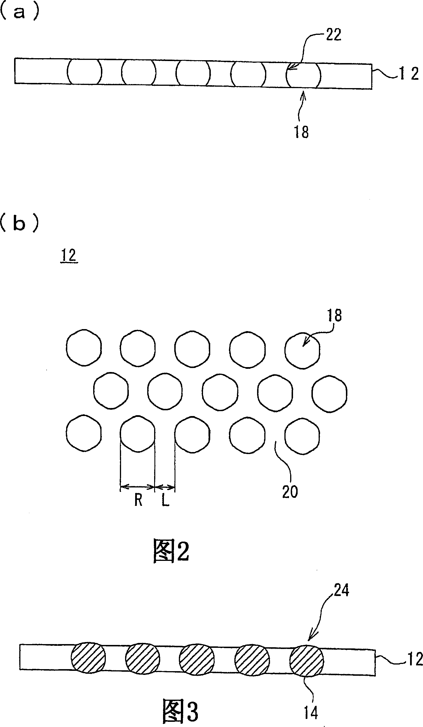
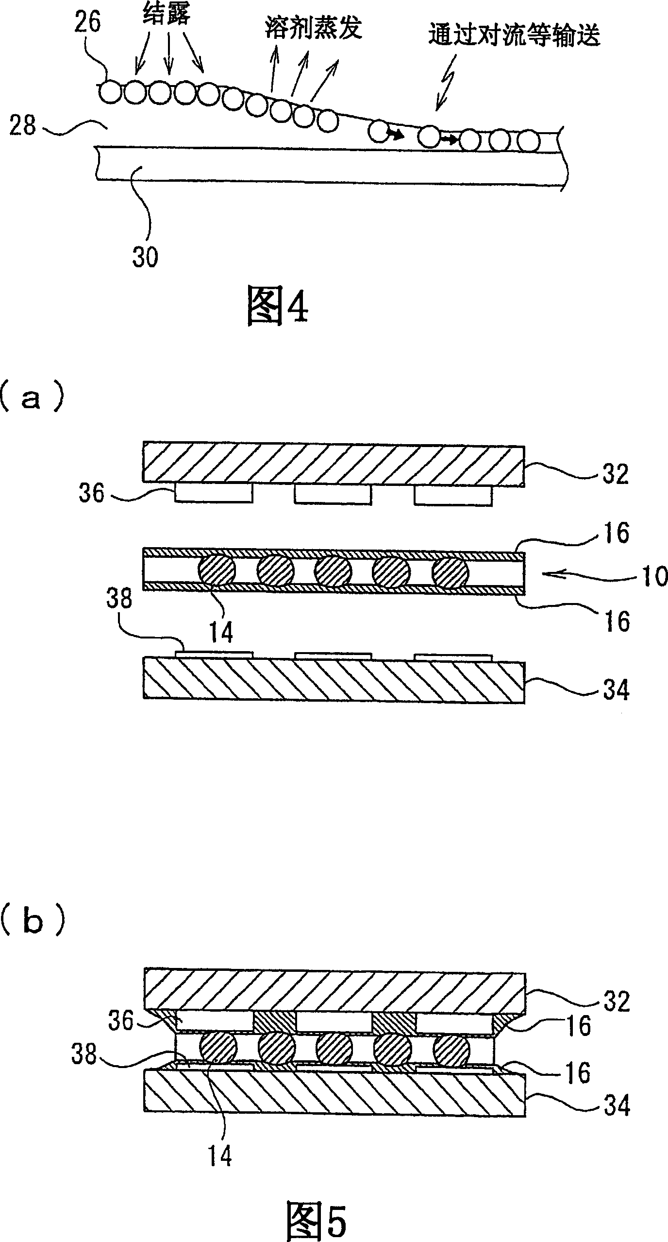
[0143] Then, the polymer solution was cast to a coating film thickness of 780 [μm] on a shallow pan (φ90 [mm]) continuously sprayed with air at a relative humidity of 50%, and the chloroform was volatilized. As a result, as shown in FIG. 6 , a porous membrane made of polysulfone was obtained which had many pores penetrating in the film thickness direction, the pores were arranged in a honeycomb shape, and the inner walls of the pores were curved outward. In addition, the pore diameter of the pores of the porous membrane was about 5 μm.
[0144]Then, the above-mentioned porous membrane was immersed in an Ag ethanol dispersion solution having a concentration of 3 [wt%]...
Embodiment 2
[0148] Polysulfone was dissolved in chloroform at a concentration of 0.2 [wt%], and the coating film thickness was set to 1560 [μm]. In the same manner as in Example 1, the anisotropic conductive film of Example 2 was produced. membrane. The porous membrane made of polysulfone obtained when the anisotropic conductive membrane of Example 2 was produced, and the porous membrane filled with Ag particles in the pores are shown in FIGS. 8 and 9 , respectively. In addition, the pore diameter of the pores of the porous membrane was about 10 μm.
Embodiment 3
[0150] Instead of polysulfone, siloxane-modified polyimide (manufactured by Ube Industries, "R15") was dissolved in chloroform at a concentration of 0.1 [wt%]. The anisotropic conductive film of Example 3 was produced in the same manner as in Example 1 except that the speed was set at 7 [μm / sec]. The porous film made of siloxane-modified polyimide obtained when the anisotropic conductive film of Example 3 was produced, and the porous film filled with Ag particles in the pores are shown in FIGS. 10 and 11, respectively. . In addition, the pore diameter of the pores of the porous membrane was about 5 μm.
PUM
| Property | Measurement | Unit |
|---|---|---|
| particle size | aaaaa | aaaaa |
| pore size | aaaaa | aaaaa |
Abstract
Description
Claims
Application Information