

Tantalum carbide-covered carbon material and process for producing the same
A technology of tantalum carbide and carbon materials, applied in the direction of gaseous chemical plating, metal material coating process, coating, etc., can solve the problems of reduced softness, easy cracks, and shortened life of carbon materials, so as to achieve inhibition of release, Effect of reducing corrosion, reducing cracks and peeling
- Summary
- Abstract
- Description
- Claims
- Application Information
AI Technical Summary
Problems solved by technology
Method used
Image

Examples
Embodiment 1~3
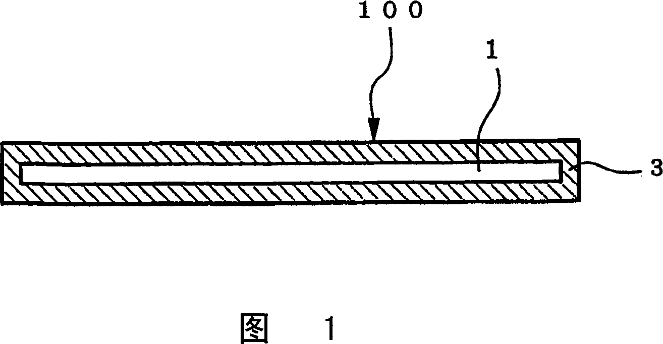
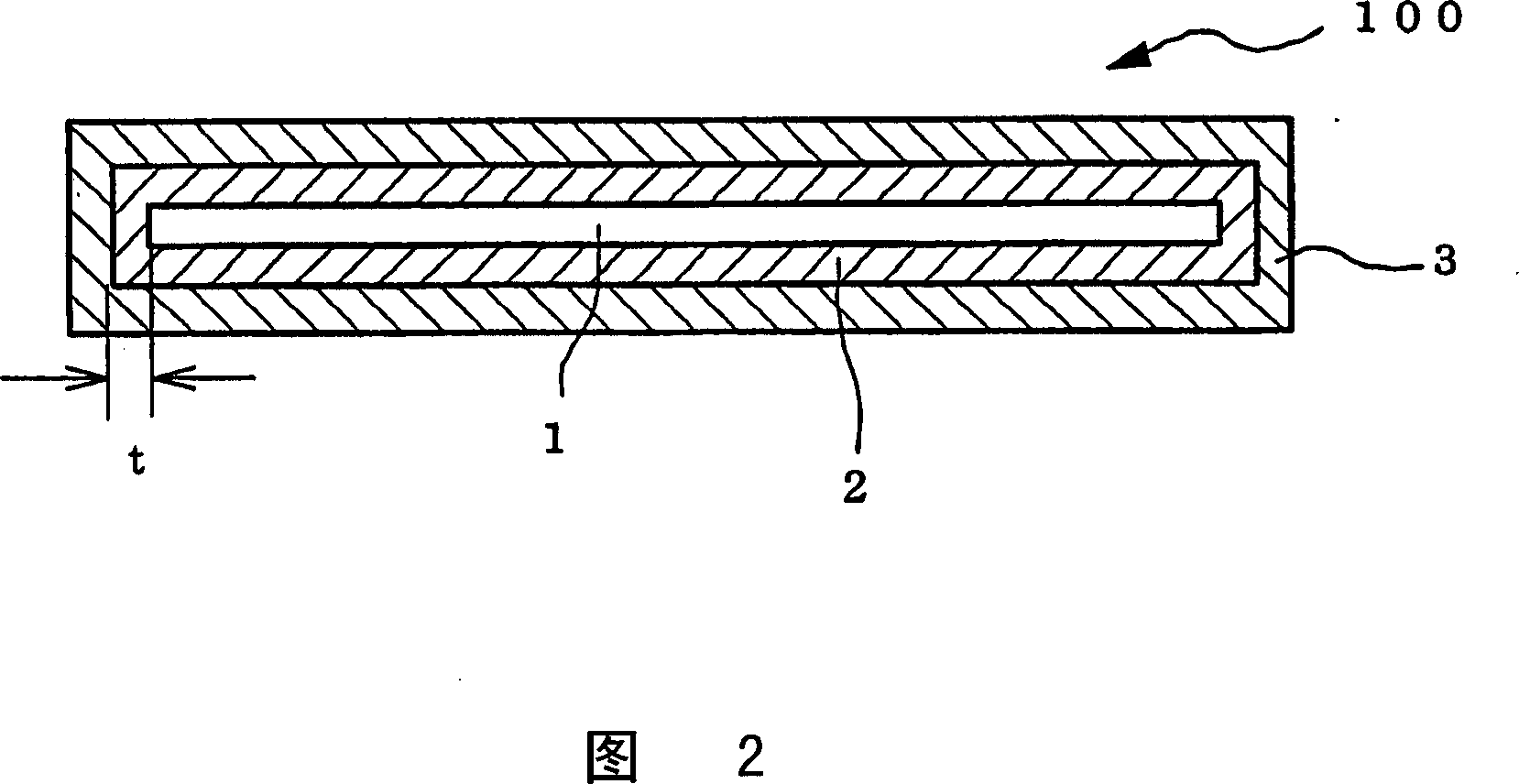
[0106] Set the thermal expansion coefficient to 7.8×10 -6 / K, the gas release pressure based on 1000℃ is 10 -6 A graphite substrate with a diameter of 66 mm and a thickness of 10 mm with Pa / g and an ash content of 2 ppm was subjected to the above halogen treatment, and then a tantalum carbide coating film was formed on the carbon substrate under the CVD conditions shown in Table 1 below. At this time, the C / Ta composition ratio of the coating film passes C 3 H 8 Adjust the flow rate to 1.0~1.2. Using the CVD conditions shown in Table 1, the film thickness was changed to 21, 34, and 44 μm by changing the reaction time to 11, 18, and 25 hours. Then, heat treatment was further performed at 2000° C. for 10 hours in a hydrogen atmosphere to further improve the crystallinity of the coating film 3. The X-ray diffraction results of Examples 1 to 3 are shown in Figs. 15 to 17. In X-ray diffraction, the diffraction lines of the (220) plane were mainly confirmed, and the diffraction lines of...
Embodiment 4~8
[0112] The tantalum carbide coating film 3 was formed by the CVD method on the same carbon substrate 1 as used in Examples 1 to 3. The CVD conditions are: temperature is fixed at 850℃, pressure is fixed at 1330Pa, and C is changed 3 H 8 And TaCl 5 The flow rate of tantalum carbide changes in the range of 1-30μm / hr. In Examples 4 to 6, after the coating film 3 was formed, it was heat-treated in a hydrogen atmosphere at 2000° C. for 10 hours. The crystal structure of the coating film 3 was detected by X-ray diffraction. As a result, the intensity ratio of the (220) plane diffraction line was the strongest, which was 4 times or more than the intensity of the second strong diffraction line. As shown in Table 3, the half-value width of the diffraction line of the (220) plane of the coating film 3 is in the range of 0.11 to 0.14°. Such a coating film will not crack or peel before the thermal shock test in a reducing gas atmosphere, which is ideal. In particular, the coating film exhibit...
Embodiment 9~18
[0116]The carbon material 100 was manufactured using various graphite substrates 1 having the characteristics shown in Table 4. The halogen treatment was performed on a graphite substrate having various coefficients of thermal expansion (CTE) shown in Table 4 with a diameter of 60 mm and a thickness of 10 mm, so that the ash content of the graphite substrate was 10 ppm or less. However, in Example 18, the halogen treatment was omitted, and the ash content of the graphite substrate 1 was 16 ppm. A tantalum carbide coating film 3 (thickness 43 μm) was formed on the substrate under the same conditions as in Examples 1 to 3. The composition ratio of C / Ta of the coating film 3 passes C 3 H 8 The flow rate is adjusted to 1.0~1.2. After the coating film 3 is formed, heat treatment is performed at 2000° C. for 10 hours in a hydrogen atmosphere. The (220) plane of the coating films of Examples 9 to 18 all showed the strongest diffraction intensity, and the intensity was 4 times or more tha...
PUM
| Property | Measurement | Unit |
|---|---|---|
| thickness | aaaaa | aaaaa |
| thickness | aaaaa | aaaaa |
| density | aaaaa | aaaaa |
Abstract
Description
Claims
Application Information