Array base board structure of thin film transistor liquid crystal display and its producing method

An array substrate structure and thin-film transistor technology, which is applied in semiconductor/solid-state device manufacturing, transistors, static indicators, etc., can solve the problems of low yield rate and high cost, achieve simplified manufacturing process, increase contact area, and optimize ground clearance The effect of the stripping process

Active Publication Date: 2007-06-27
BEIJING BOE OPTOELECTRONCIS TECH CO LTD +1
View PDF0 Cites 41 Cited by
  • Summary
  • Abstract
  • Description
  • Claims
  • Application Information

AI Technical Summary

Problems solved by technology

The above defects have caused disadvantages such

Method used


Image

  • Array base board structure of thin film transistor liquid crystal display and its producing method
  • Array base board structure of thin film transistor liquid crystal display and its producing method
  • Array base board structure of thin film transistor liquid crystal display and its producing method

Examples


Embodiment Construction

[0034] Below in conjunction with accompanying drawing and specific embodiment, the present invention is described in further detail:

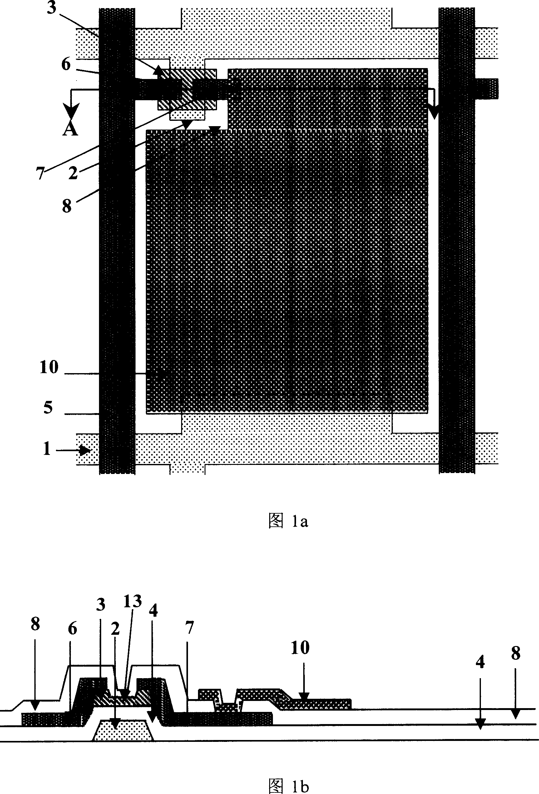
[0035] First, use the first mask plate to form the gate scan line 1 and the gate electrode 2 on the glass substrate: Referring to Figure 5a and Figure 5b, the first mask is formed on the glass substrate by magnetron sputtering or other film forming methods. A layer of metal film, that is, gate metal film. The material of the gate metal thin film may be metals such as molybdenum, aluminum, aluminum-nickel alloy, tungsten, chromium, or copper, or an alloy of the above-mentioned metal materials. In some cases, it can also be a multi-layer film structure, and the material of each layer of film can be selected from the above materials. Next, the first mask is used to form patterns of the gate scan line 1 and the gate electrode 2 through photolithography and etching processes.

[0036] Then, a second mask is used to form patterns of gate insulating...


PUM


Abstract

Through enlarging contact area between transparent pixel electrode and drain electrode of thin film transistor (TFT), structure of array base plate (ABP) of TFT LCD form favorable connection. The method for preparing ABP of TFT LCD includes three steps of photoetching technology with masks: first, using first ordinary mask defines pattern of first layer of metal thin film so as to form grid scan lines, and grid electrode; then, using second mask i.e. graytone, semitransparent mask defines patterns of second layer of metal thin film and active layer to form channels of data scan lines, silicon island, source/drain electrodes and TFT; finally, using third ordinary mask defines second layer of insulation film i.e. pattern of passive film, and using lift off stripping technique forms patterns of transparent conductive film, i.e. transparent pixel electrodes. The invention reduces number of mask, and number of photoetching process, and simplifies procedure for preparing ABP of TFT LCD.

Description

technical field [0001] The invention relates to an array substrate structure of a thin film transistor liquid crystal display (TFT-LCD) and a manufacturing method thereof. Background technique [0002] Liquid crystal display technology is developing very fast, and due to its light weight, liquid crystal display devices are widely used in portable electronic devices. With the expansion of application fields, cost reduction and productivity improvement in manufacturing technology are required. The manufacture of a liquid crystal display device is completed by a series of thin film deposition and photolithography process to form a pattern. The number of masks used in lithography is a measure of the complexity of the manufacturing process of liquid crystal display devices. One photolithography process uses one mask. Many researchers have investigated possible ways to reduce the number of reticles, because one less reticle means lower manufacturing costs. [0003] Usually a l...

Claims


Application Information

Patent Timeline
IPC IPC(8): G02F1/136G02F1/133H01L29/786H01L21/027G03F7/20
Inventor 龙春平
Owner BEIJING BOE OPTOELECTRONCIS TECH CO LTD
Why Eureka
Try Eureka