
THz signal highly-sensitive detector and camera

A high-sensitivity, detector technology, applied in the direction of instruments, optics, camera bodies, etc., can solve the problems of low spatial-temporal resolution, slow scanning time, and low detection sensitivity, and achieve high sensitivity, good integration performance, and time-resolved Good rate effect

Inactive Publication Date: 2007-07-11
欧阳征标 +1
View PDF1 Cites 13 Cited by
  • Summary
  • Abstract
  • Description
  • Claims
  • Application Information

AI Technical Summary

Problems solved by technology

A disadvantage of this method is that there is a scanning upper limit, the scanning time is too slow, the observed spectral information is not timely enough, and the spatial and temporal resolution is very low, making it difficult to achieve real-time imaging
In addition, because the scan speed is too slow, it is a slow scan time delay measurement, which cannot effectively suppress thermal background noise
This makes THz imaging technology unable to be applied in practice. For example, image signals need to be obtained immediately in customs inspection or security inspection in confidential places, which requires the development of practical THz detectors and cameras.
[0010] In addition, most of the current THz detection and imaging technologies are implemented using electro-optic modulation components, which also hinders the development of THz detectors and cameras in the direction of integration.
[0011] The document "Tahertz wave two-dimensional electro-optic array imaging method" with patent number 03116029.8 introduces a two-dimensional array electro-optic crystal THz signal detector. Imaging once, but its detection sensitivity is not high, and its ability to detect low-power THz signals is relatively poor

Method used


Image

  • THz signal highly-sensitive detector and camera
  • THz signal highly-sensitive detector and camera

Examples


Embodiment Construction

[0021] The present invention will be further described below in conjunction with accompanying drawing.

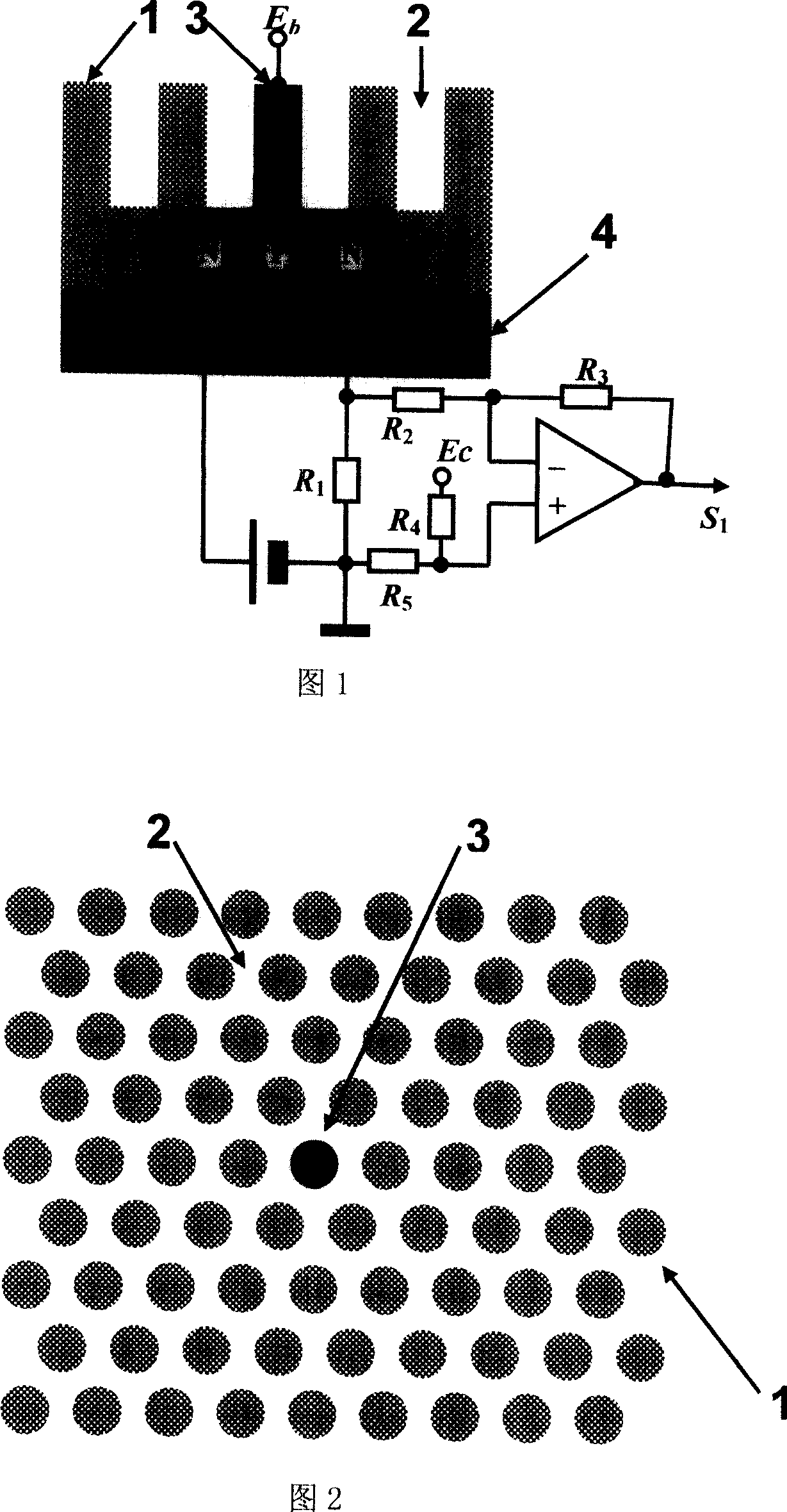
[0022] The semiconductor material Si is chosen to fabricate the photonic crystal microcavity. Referring to FIG. 1 , semiconductor Si is grown on a ceramic substrate 4 by molecular beam epitaxy. Photonic crystals are fabricated on Si substrates by etching techniques. 1 is the high refractive index medium Si, and 2 is the low refractive index medium air. The lattice constant of the photonic crystal is of the same order of magnitude as the wavelength of THz light, which can be selected as 10 μm. By changing the duty cycle of the medium 1, the band gap of the photonic crystal can be adjusted to move in the THz wavelength range. By changing the size of one of the high-refractive-index media and forming the defect region 3, a photonic crystal THz microcavity can be obtained. Fig. 2 is a top view of the photonic crystal microcavity. By adjusting the radius of the defect regio...


PUM


Abstract

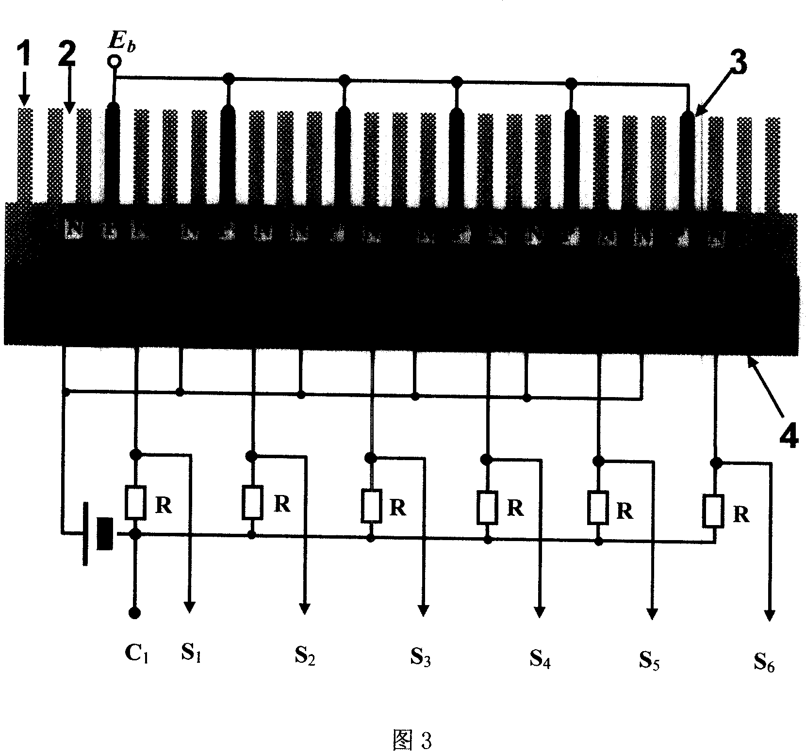
The structure of THz signal high sensitivity detector and detecting head is as follows. It makes association of photon crystal THz micro cavity and semi conductor transistor on the base of the semiconductor. It generates big density of field energy of the micro cavity when the THz wave injects, the generated thermal effect will make electric hollow cavity pair, amplifies the carrier after flowing into the base of the transistor, generating current of the outside circuit, to detect THz signal to realize high sensitivity THz signal detection. It accumulates several detectors to form a THz harmonic matrix, with each harmonic cavity receiving specific location, and intensity of THz light. Being amplified and stored, the signal can get a complete THz image to realize timely photo taking function. It uses special signal amplification circuit to realize elimination of background THz radiation noise.

Description

(1) Technical field [0001] The invention relates to a high-sensitivity THz signal detector and camera, in particular to a THz signal high-sensitivity detector and camera using photonic crystals. (2) Background technology [0002] THz waves generally refer to electromagnetic radiation with a frequency in the range of 100 GHz to 10 THz (30 μm to 3 mm), and its wave band is between microwave and infrared light. Due to the lack of effective THz generation and detection methods before, people's understanding of the properties of electromagnetic radiation in this band is so limited that this band has long been called the "THz gap" in the electromagnetic spectrum. In the past ten years, the rapid development of ultrafast laser technology has provided a stable and reliable excitation light source for the generation of THz pulses, and promoted the vigorous development of THz wave radiation mechanism research, detection technology and application technology. [0003] Compared with tr...

Claims


Application Information

Patent Timeline
Patent Type & Authority Applications(China)
IPC IPC(8): G01R29/08G01R29/10
CPCG03B17/00
Inventor 欧阳征标
Owner 欧阳征标
Learn More