Method of making a photonic crystal device and photonic crystal device

a technology of photonic crystal and oled, which is applied in the field of making a photonic crystal device, can solve the problems of poor external efficiency of the device, inability to capture all or nearly all of the light produced, and the light output of the emissive elements of the oled is trapped within the device, etc., and achieves the effect of efficiently extracting the light from the devi

Active Publication Date: 2020-06-23
BRAGGONE
View PDF28 Cites 0 Cited by
  • Summary
  • Abstract
  • Description
  • Claims
  • Application Information

AI Technical Summary

Benefits of technology

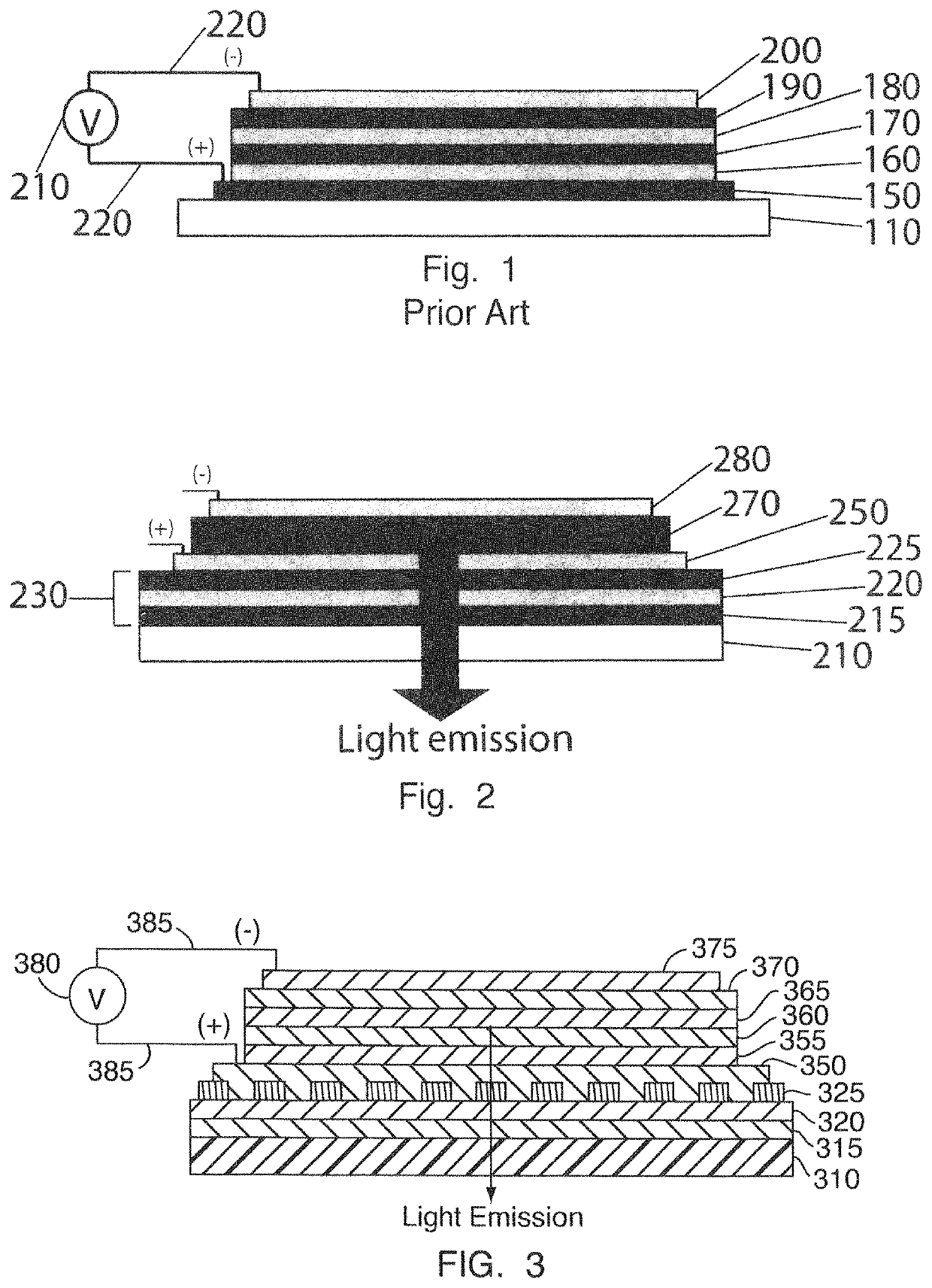
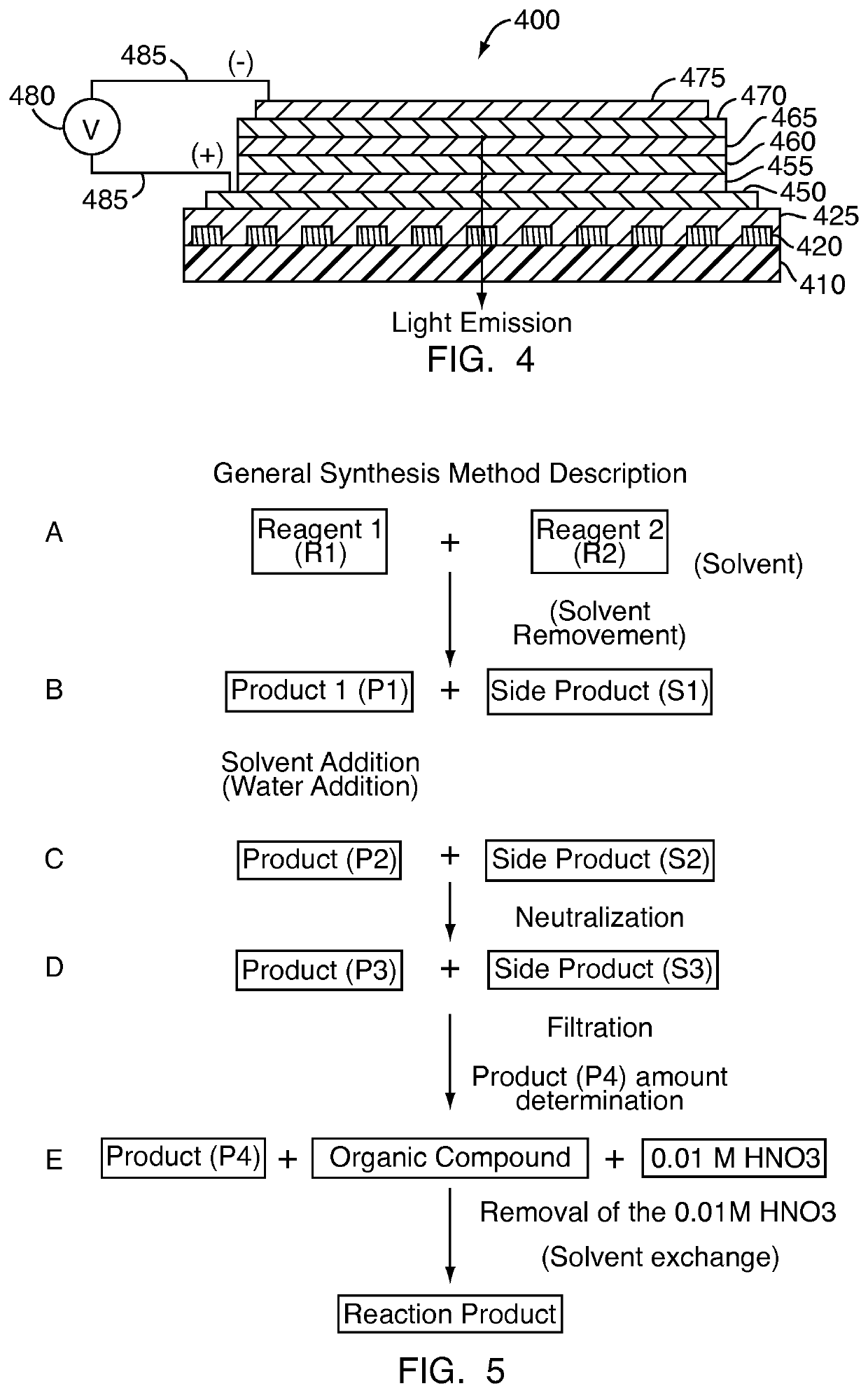
[0010]The present invention is based on the idea of providing a light emitting diode (OLED) device which contains a substrate with a photonic crystal, whereby the formed film structure induces enhancement of the liberation of photons trapped inside the light emitting device structure.
[0015]Considerable advantages are obtained by the invention. Thus, the light trapped due to total internal reflection in a waveguide acting light emitting structure can be extracted efficiently from the device by introducing the photonic crystal device structure between the substrate and conductive anode layer.

Problems solved by technology

However, as is well known, much of the light output from the emissive elements in the OLED is trapped within the device.
In general, up to 80% of the light may be lost leading to poor external efficiency of the device.
However, none of these approaches capture all, or nearly all, of the light produced.
This approach is not compatible and practical with the current manufacturing techniques used to make OLED displays, since for bottom-emitting OLED displays, manufacturing starts with a glass substrate that is coated with a layer of conductive indium tin oxide (ITO) which is patterned to provide conductors for thin-film transistors located on the substrate.
The use of photoresists for creating plasmon inducing gratings is problematical because the photoresist is an electrical insulator, thereby isolating the underlying ITO conductors from the OLED materials.
The use of shadow masks is not a practical way to create the gratings because of the small dimensions of the gratings.

Method used


Image

  • Method of making a photonic crystal device and photonic crystal device
  • Method of making a photonic crystal device and photonic crystal device
  • Method of making a photonic crystal device and photonic crystal device

Examples


polymer example i

brid Polymer 1

[0132]Ti(iOPr)4 (0.05277 mol) was placed in a round bottom flask.TiCl4 (0.05277 mol) was added by syringe and needle. The solution containing a white solid was stirred at room temperature (RT) for 10 min. 125.04 g of 2-isopropoxyethanol was added and the clear yellow solution was stirred at room temperature for 30 min. (Nd=1.4332). 3.80 g of H2O (0.21099 mol) was added and the reaction solution was stirred at room temperature for an additional 5 min (Nd 1.4322). 21.36 g of TEA (0.211088 mol) was added to neutralize the reaction mixture. The obtained white suspension was stirred at room temperature for 2 h. The white reaction suspension was filtrated using pressure filter (filter paper size 0.45 um) Nd=1.4235 and pH=6.5-7 (pH-paper was used for determination). The amount of material in grams after filtration was 92.71 g. An acidic water solution (nitric acid, HNO3, 0.0652 mol) was added to the reaction mixture. Then, metacrylic acid (MAA, 0.1304 mol) was added dropwise ...

polymer example ii

rid Polymer 1

[0133]TaCl5 (0.007342 mol) was placed to a round bottom flask and methanol (MeOH) (26 ml) was added. To the clear reaction solution Ta(OEt)5 (0.007342 mol) was added. The clear reaction solution was stirred at room temperature for 2 h. Solvent exchange from MEOH to 2-isopropoxyethanol (5×) was carried out using rotary evaporator (p=200-51 mbar, tbath=40° C.). The clear reaction solution was stirred at room temperature for a few minutes and after that the reaction solution was neutralized using TEA (m=4.62 g; 0.04566 mol). The white suspension was stirred at room temperature for 2 h and then filtrated using pressure filter (0.45 um). The clear solution obtained was placed in freezer overnight. After this the suspension was filtrated. The solvent used during the synthesis was removed by rotary evaporator (p=100-1 mbar, t(bath)=40° C., at 1 mbar for 10 min). 6.82 g of IPA:MeOH:1-butanol solution (6:3:1) was added as processing solvent to the material. Clear reaction soluti...

polymer example iv

1

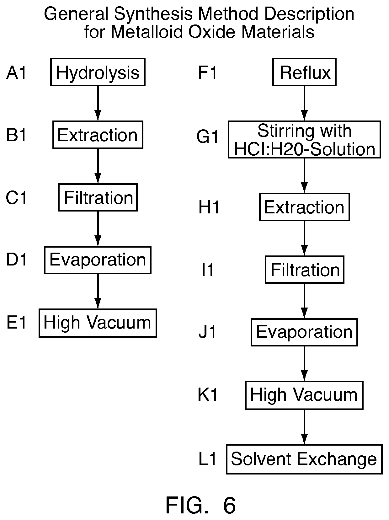
[0150]Trifluoropropyltrichlorosilane (26.38 g, 0.1139 mol) and allyltrichlorosilane (13.32 g, 0.07596 mol) were weighed to a round bottom flask. 183 g of dichloromethane (DCM) was added. This clear DCM solution was added using a dropping funnel to another flask in an ice bath containing a DCM:H2O solution 23 ml:160 ml. The DCM solution was added in 60 min. The temperature was maintained during addition between 2-5° C. After addition, the reaction mixture was stirred at room temperature (RT) for 120 min. After this the reaction mixture was placed in a separation funnel and 120 g of DCM was added. The DCM and H2O layers were separated. The DCM phase was extracted six (6) times using 65 ml of distilled water in each extraction run. The pH of the DCM-phase was, after the last extraction, neutral. The DCM-layer was filtrated once using a filter paper. DCM was removed by evaporation (p=400-2 mbar, T(bath)=40° C.). The vacuum was maintained below 18 mbar for 5 min. After this, the clear m...


PUM

PropertyMeasurementUnit
wavelengthaaaaaaaaaa
work functionaaaaaaaaaa
refractive indexaaaaaaaaaa

Abstract

The invention is based on the idea of providing a light emitting diode (OLED) device which contains a substrate with a photonic crystal, whereby the formed film structure induces enhancement of the liberation of photons trapped inside the light emitting device structure. The photonic crystal structure is a film structure on a substrate produced using a combination of high and low refractive index materials, at least one of the materials being based on a liquid phase deposited metal-oxide or metalloid oxide material. By means of the invention light trapped due to total internal reflection in a waveguide acting light emitting structure can be extracted efficiently from the device by introducing the photonic crystal device structure between the substrate and conductive anode layer.

Description

CROSS REFERENCE TO RELATED APPLICATIONS[0001]This application is entitled to the benefit of and incorporates by reference essential subject matter disclosed in International Patent Application No. PCT / FI2006 / 000209 filed on Jun. 15, 2006 and U.S. Provisional Application No. 60 / 691,315 filed Jun. 15, 2005.BACKGROUND OF THE INVENTIONField of the Invention[0002]The present invention is based on the idea of providing a light emitting diode (OLED) device that includes a substrate with a photonic crystal, whereby the formed film structure induces enhancement of the liberation of photons trapped inside the OLED device structure and substrate.Description of Related Art[0003]Organic light emitting diodes (OLED) have shown great promise for flat-panel displays and as alternative solid state illumination sources. This technology relies upon thin-film layers of materials coated on a substrate. However, as is well known, much of the light output from the emissive elements in the OLED is trapped ...

Claims


Application Information

Patent Timeline
Patent Type & Authority Patents(United States)
IPC IPC(8): H01L51/52G02B6/122B82Y20/00
CPCB82Y20/00G02B6/1225H01L51/5275H10K50/858
Inventor KARKKAINEN, ARI
Owner BRAGGONE
Why Eureka
Try Eureka