
Active matrix organic light-emitting diode display device and method of manufacturing the same

Active Publication Date: 2022-01-25
IND ACADEMIC COOP FOUNDATION YONSEI UNIV
View PDF22 Cites 0 Cited by
  • Summary
  • Abstract
  • Description
  • Claims
  • Application Information

AI Technical Summary

Benefits of technology

The present patent text describes an active matrix organic light-emitting diode display device with a transition metal chalcogenide based backplane that forms an insulating layer with a high dielectric constant or permittivity to simultaneously lower channel resistance and contact resistance. The device can be used in various fields, such as medical or sports, and is reliable and uniform. The invention also reduces roughness of the substrate or scattering effect due to charges trapped by the substrate, thereby effectively reducing hysteresis. Additionally, the invention is applicable to wearable or flexible devices.

Problems solved by technology

When the transition metal chalcogenides are manufactured by a mechanical peeling method, only pieces having a very small area can be formed so that there is a limit to implement large-area electronic devices.
However, the transition metal chalcogenides grown using the chemical vapor deposition have a difficulty to be applied to a backplane for a flexible system or a large area organic light-emitting diode display due to a low mobility and an inferior semiconductor characteristic caused by a small crystal grain boundary.

Method used


Image

  • Active matrix organic light-emitting diode display device and method of manufacturing the same
  • Active matrix organic light-emitting diode display device and method of manufacturing the same
  • Active matrix organic light-emitting diode display device and method of manufacturing the same

Examples


example

(Synthesis of Molybdenum Disulfide (MoS2))

[0123]A double layered molybdenum disulfide was grown using MOCVD. A 4-inch Si wafer containing thermally grown SiO2 with a thickness of 300 nm was placed in a quartz tube with a 4.3-inch diameter.

[0124]Before growing molybdenum disulfide, washing was performed with water, acetone, and isopropanol to remove organic materials or impurities that may have formed on the surface of the SiO2 / p+-Si substrate.

[0125]Molybdenum hexacarbonyl (WIC; 577766, Sigma-Aldrich) and dimethylsulfide (DMS; 471577, Sigma-Aldrich) with a high equilibrium vapor pressure were selected as precursors of Mo and S, respectively, and H2 and Ar were used as gaseous carrier gases.

[0126]The double-layered molybdenum disulfide was grown with a condition of a pressure of 7.5 torr, a growth temperature of 550° C., a growth time of 20 hours, a MHC flow rate of 1.0 sccm per minute, a DMS flow rate of 0.3 sccm, and a flow rate of H2 and Ar of 300 sccm and 10 sccm.

(To Form Molybden...


PUM


Abstract

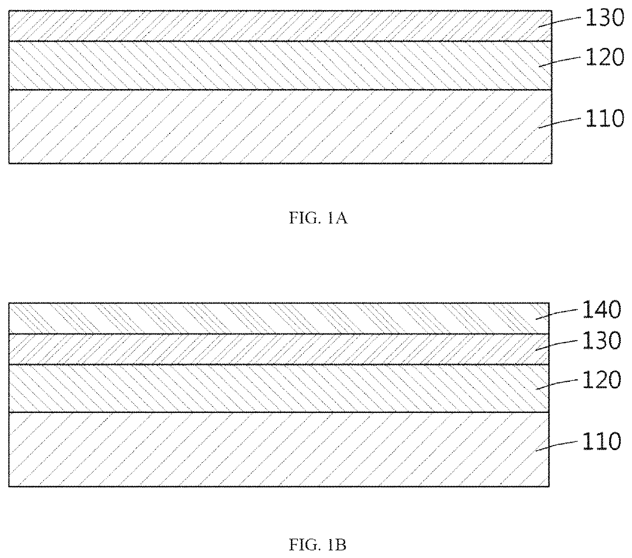
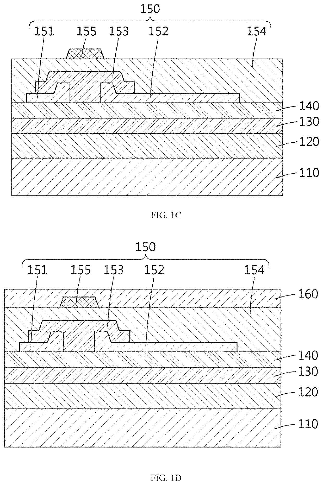
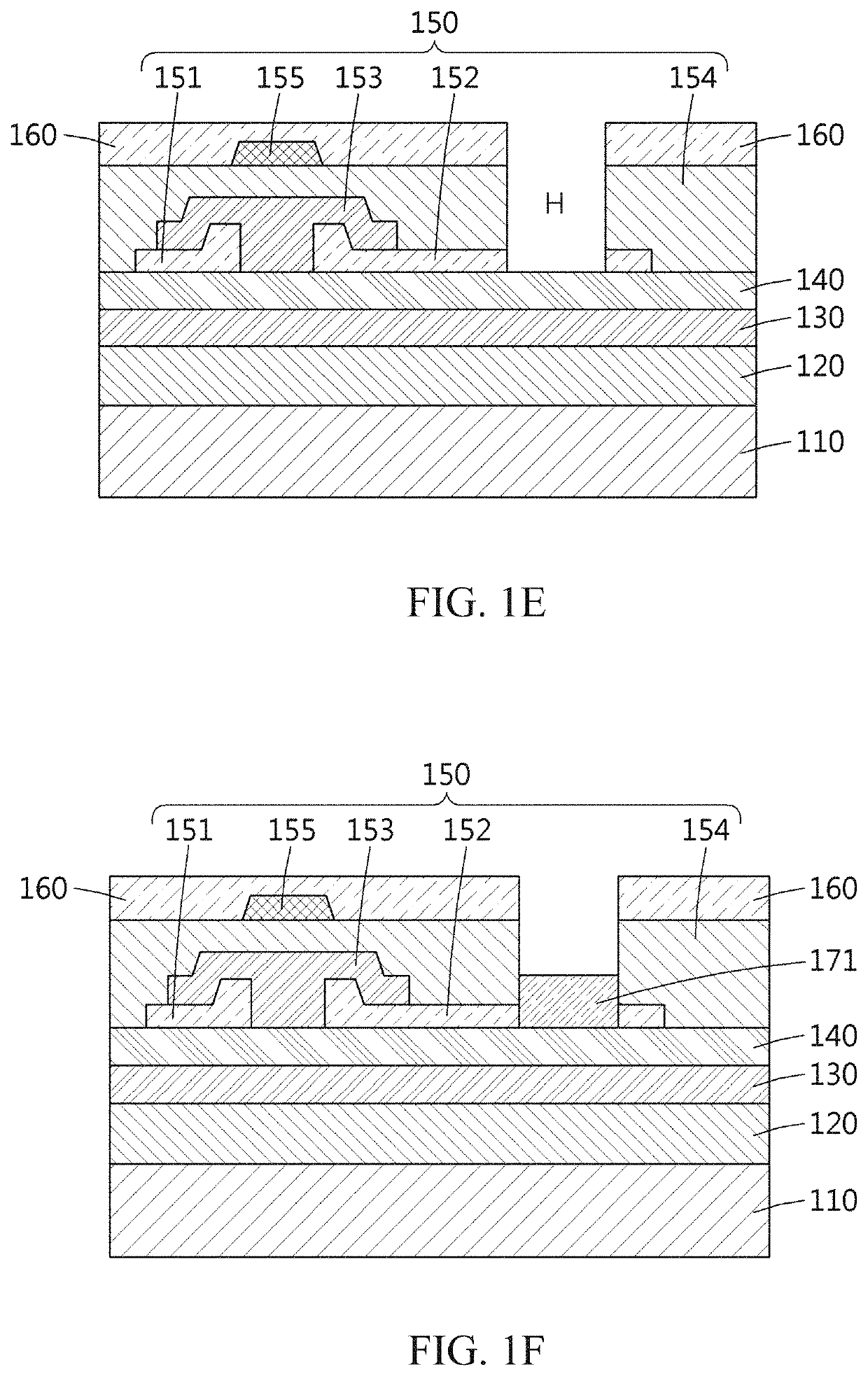
The present disclosure discloses an active matrix organic light-emitting diode display device and a manufacturing method thereof. The method includes forming a sacrificial layer on a carrier layer; forming a flexible substrate on the sacrificial layer; forming a first insulating layer on the flexible substrate; forming at least one transition metal chalcogenide based backplane on the first insulating layer; and forming an opening unit after forming a capping layer on the at least one transition metal chalcogenide based backplane; and forming at least one active matrix organic light-emitting diode unit which is electrically connected to the at least one transition metal chalcogenide based backplane in the opening unit.

Description

CROSS-REFERENCE TO RELATED APPLICATIONS[0001]This application is a U.S. National Stage of PCT / KR2019 / 004822, filed on Apr. 22, 2019, which claims priority to and the benefit of Korean Patent Application No. 10-2018-0117746 filed in the Korean Intellectual Property Office on Oct. 2, 2018, the entire contents of which are incorporated herein by reference.TECHNICAL FIELD[0002]The present disclosure relates to an active matrix organic light-emitting diode display device and a method of manufacturing the same, and more particularly, to an active matrix organic light-emitting diode display device which includes a transition metal chalcogenide based backplane including a channel layer interposed between dielectric layers having a high permittivity to improve electron mobility and reduce both a channel resistance and a contact resistance and a method of manufacturing the same. This research relates to the center for strain engineered electronic devices in the leader researcher support proje...

Claims


Application Information

Patent Timeline
IPC IPC(8): H01L27/32H01L51/00H01L51/56H01L29/786H01L27/12
CPCH01L27/3262H01L27/3248H01L29/78681H01L51/0097H01L51/56H01L27/1225H01L2227/323H01L2227/326H01L2251/5338Y02P70/50H01B3/02Y02E10/549H10K59/123H10K2102/311H10K77/111H01B3/025H10K59/1213H10K71/00H10K59/1201H10K71/80
Inventor AHN, JONG HYUNKIM, SOO YOUNGCHOI, MIN WOOPARK, YONG JUSHARMA, BHUPENDRA KUMARBAE, SA RANG
Owner IND ACADEMIC COOP FOUNDATION YONSEI UNIV
Learn More