Methods and systems for semiconductor metrology based on polychromatic soft X-Ray diffraction

a polychromatic soft x-ray diffraction and metrology technology, applied in semiconductor/solid-state device testing/measurement, material analysis using wave/particle radiation, instruments, etc., can solve the problems of limited information concerning the composition and shape of nanostructures, difficult characterization, and inability to accurately determine the composition of materials, etc., to achieve the effect of improving the measurement throughpu

Active Publication Date: 2022-05-17
KLA CORP
View PDF70 Cites 3 Cited by
  • Summary
  • Abstract
  • Description
  • Claims
  • Application Information

AI Technical Summary

Benefits of technology

[0017]RSAXS measurements of a semiconductor wafer are performed over a range of wavelengths, angles of incidence, and azimuth angles with a small illumination beam spot size (e.g., less than 50 micrometers across the effective illumination spot). In one aspect, the RSAXS measurements are performed with x-ray radiation in the soft x-ray (SXR) region (i.e., 80-3000 eV) at grazing angles of incidence in the range of 5-20 degrees. Grazing angles for a particular measurement application are selected to achieve a desired penetration into the structure under measurement and maximize measurement information content with a small beam spot size (e.g., less than 50 micrometers).
[0020]The x-ray illumination source of an RSAXS metrology system produces x-ray emission over a source area having finite lateral dimensions (i.e., non-zero dimensions orthogonal to the beam axis. In one aspect, the source area of illumination source 110 is characterized by a lateral dimension of less than 20 micrometers. In some embodiments, the source area is characterized by a lateral dimension of 10 micrometers or less. Small source size enables illumination of a small target area on the specimen with high brightness, thus improving measurement precision, accuracy, and throughput.
[0023]In another further aspect, an RSAX metrology system includes one or more beam slits or apertures to shape the x-ray illumination beam 114 incident on a specimen and selectively block a portion of illumination light that would otherwise illuminate a metrology target under measurement. One or more beam slits define the beam size and shape such that the x-ray illumination spot fits within the area of the metrology target under measurement. In addition, one or more beam slits define illumination beam divergence to minimize overlap of diffraction orders on the detector.
[0025]In some embodiments, a combined metrology tool includes a multiple wavelength SXR diffraction subsystem as described herein and an x-ray reflectometry subsystem to improve measurement throughput. In one embodiment, the multiple wavelength SXR diffraction subsystem and the x-ray reflectometry subsystem employ orthogonal planes of incidence that enable simultaneous measurements or sequential measurements without having to move the specimen under measurement or either of the optical measurement subsystems.

Problems solved by technology

As devices (e.g., logic and memory devices) move toward smaller nanometer-scale dimensions, characterization becomes more difficult.
Devices incorporating complex three-dimensional geometry and materials with diverse physical properties contribute to characterization difficulty.
Accurate information concerning the material composition and shape of nanostructures is limited in the process development environment of a leading-edge front-end semiconductor fabrication facility.
With limited knowledge of material composition and shape of nanostructures available apriori, measurement recipe development and validation is a slow and tedious process.
For example, cross-sectional transmission electron microscopy (TEM) images are used to guide optical scatterometry model development, but TEM imaging is slow and destructive.
Furthermore, when absorbing materials are present in the structure under measurement, penetration and scattering of illumination light in the optical region (e.g., 0.5-10 ev) limits the utility of conventional optical metrology systems.
Similarly, electron beam based metrology systems struggle to penetrate semiconductor structures due to absorption and scattering of the illuminating, backscattered, and secondary emission electrons.
Atomic force microscopes (AFM) and scanning-tunneling microscopes (STM) are able to achieve atomic resolution, but they can only probe the surface of the specimen.
In addition, AFM and STM microscopes require long scanning times that make these technologies impractical in a high volume manufacturing (HVM) setting.
Scanning electron microscopes (SEM) achieve intermediate resolution levels, but are unable to penetrate structures to sufficient depth.
Thus, high-aspect ratio holes are not characterized well.
In addition, the required charging of the specimen has an adverse effect on imaging performance.
However, scattering of hard x-rays from shallow structures, e.g., logic metrology applications, is weak, which severely limits achievable measurement resolution and throughput.
As such, T-SAXS has not been shown to be a viable option for logic metrology applications in an HVM environment.
These scaling factors impose a strong penalty on T-SAXS systems for metrology of shallow structures.
Typically, within the context of a complex high volume manufacturing environment, it is very difficult to obtain and manage the required metrology and process information.
This is so large that even scribe-line metrology targets are unuseable.
This loss of functional wafer real estate is costly.
In addition, the surface sensitivity of GI-SAXS measurements is excellent, but penetration of high aspect ratio structures is very limited due to evanescent field behavior.

Method used


Image

  • Methods and systems for semiconductor metrology based on polychromatic soft X-Ray diffraction
  • Methods and systems for semiconductor metrology based on polychromatic soft X-Ray diffraction
  • Methods and systems for semiconductor metrology based on polychromatic soft X-Ray diffraction

Examples


Embodiment Construction

[0035]Reference will now be made in detail to background examples and some embodiments of the invention, examples of which are illustrated in the accompanying drawings.

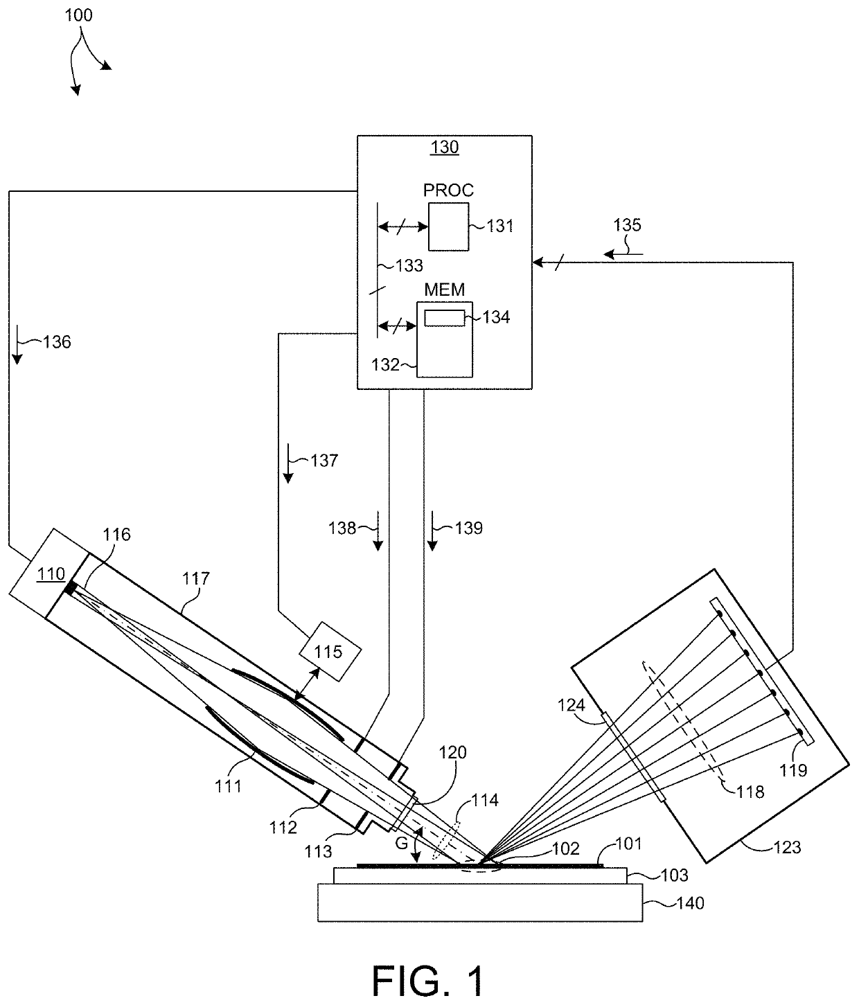
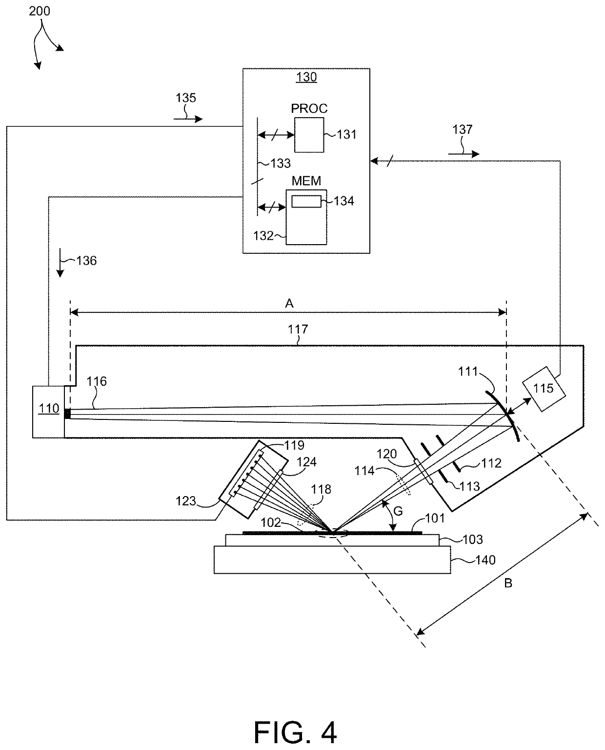
[0036]Methods and systems for measuring structural and material characteristics (e.g., material composition, dimensional characteristics of structures and films, etc.) of semiconductor structures associated with different semiconductor fabrication processes based on x-ray illumination are presented. More specifically, methods and systems for performing measurements of semiconductor structures based on high-brightness, polychromatic reflective small angle x-ray scatterometry (RSAXS) metrology are presented herein.

[0037]RSAXS measurements of a semiconductor wafer are performed over a range of wavelengths, angles of incidence, and azimuth angles with a small beam spot size (e.g., less than 50 micrometers across the effective illumination spot). In one aspect, the RSAXS measurements are performed with x-ray radiation in t...


PUM

PropertyMeasurementUnit
photon energyaaaaaaaaaa
grazing incidence angleaaaaaaaaaa

Abstract

Methods and systems for performing measurements of semiconductor structures based on high-brightness, polychromatic, reflective small angle x-ray scatterometry (RSAXS) metrology are presented herein. RSAXS measurements are performed over a range of wavelengths, angles of incidence, and azimuth angles with small illumination beam spot size, simultaneously or sequentially. In some embodiments, RSAXS measurements are performed with x-ray radiation in the soft x-ray (SXR) region at grazing angles of incidence in the range of 5-20 degrees. In some embodiments, the x-ray illumination source size is 10 micrometers or less, and focusing optics project the source area onto a wafer with a demagnification factor of 0.2 or less, enabling an incident x-ray illumination spot size of less than two micrometers. In another aspect, active focusing optics project programmed ranges of illumination wavelengths, angles of incidence, and azimuth angles, or any combination thereof, onto a metrology area, either simultaneously or sequentially.

Description

CROSS REFERENCE TO RELATED APPLICATION[0001]The present application for patent claims priority under 35 U.S.C. § 119 from U.S. provisional patent application Ser. No. 62 / 531,187, filed Jul. 11, 2017, the subject matter of which is incorporated herein by reference in its entirety.TECHNICAL FIELD[0002]The described embodiments relate to x-ray metrology systems and methods, and more particularly to methods and systems for improved measurement accuracy.BACKGROUND INFORMATION[0003]Semiconductor devices such as logic and memory devices are typically fabricated by a sequence of processing steps applied to a specimen. The various features and multiple structural levels of the semiconductor devices are formed by these processing steps. For example, lithography among others is one semiconductor fabrication process that involves generating a pattern on a semiconductor wafer. Additional examples of semiconductor fabrication processes include, but are not limited to, chemical-mechanical polishin...

Claims


Application Information

Patent Timeline
Patent Type & Authority Patents(United States)
IPC IPC(8): G01N23/201G01N23/20008H01L21/67H01L21/66
CPCG01N23/201G01N23/20008G01N2223/054G01N2223/6116H01L21/67259H01L21/67288H01L22/12G01B15/00G01B2210/56G01N2223/1016
Inventor WACK, DANIELKHODYKIN, OLEGSHCHEGROV, ANDREI V.KUZNETSOV, ALEXANDERARTEMIEV, NIKOLAYFRIEDMANN, MICHAEL
Owner KLA CORP
Why Eureka
Try Eureka