Method for manufacturing transfer film including seed layer, method for manufacturing circuit board by selectively etching seed layer, and etching solution composite

a technology of transfer film and selective etching, which is applied in the direction of liquid/solution decomposition chemical coating, printed element electric connection formation, plastic/resin/waxes insulators, etc. it can solve the problems of increasing costs, difficult to finely form an inner layer circuit, and increasing the weight of electronic products. , to achieve the effect of preventing the surface smoothness of the seed layer from being lowered, low surface smoothness, and high smoothness

Active Publication Date: 2022-09-27
INKTEC CO LTD
View PDF25 Cites 0 Cited by
  • Summary
  • Abstract
  • Description
  • Claims
  • Application Information

AI Technical Summary

Benefits of technology

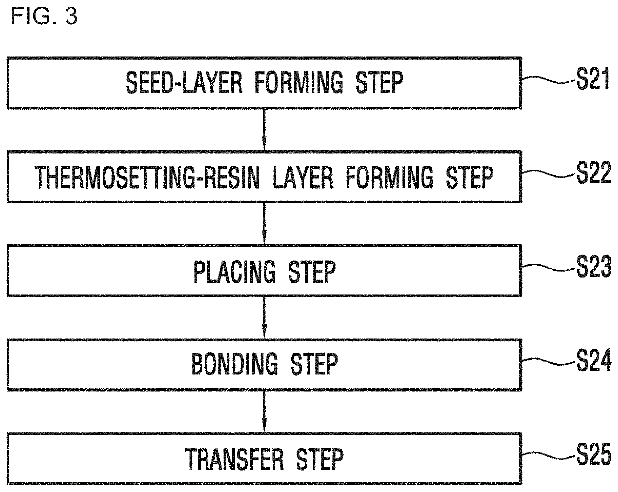
[0055]According to the present invention, there is provided a method of manufacturing a transfer film including a seed layer, in which the seed layer for forming a circuit is provided without using a copper clad film.
[0056]Further, there is provided a method of manufacturing a transfer film including a seed layer, in which a thermosetting resin layer is interposed between the seed layer and an insulating resin layer, so that a rough film having low surface smoothness can be used to form an insulating resin layer, preventing the surface smoothness of the seed layer from being lowered.
[0057]According to the present invention, there is provided a method of manufacturing a circuit board by selectively etching a seed layer, in which the seed layer having high smoothness is provided to secure high smoothness of a plating layer to be formed on the seed layer, thereby forming a precise circuit pattern.
[0058]According to the present invention, there is provided a method of manufacturing a circuit board by selectively etching a seed layer, in which the surface roughness of the seed layer is so low that diffuse reflection from the surface of the seed layer can be more suppressed than that from a copper plating layer during an exposure process for forming a pattern layer on the seed layer, thereby forming a relatively precise pattern groove and thus forming a fine circuit.
[0059]Further, according to the present invention, there is provided an etching solution composition having a high etch factor so that silver, a silver alloy or a silver compound can be selectively etched without damaging a copper circuit.
[0060]These make it possible to design a high-performance and highly-integrated circuit, and the circuit is variously applicable to a product required to be lightweight, thin, short and compact.

Problems solved by technology

However, an electronic product has gradually become lightweight and compact and has had multi and complex functions, thereby evolving into a multi-layered product of the double-sided type, the multi-layered type, etc. with high wiring density and a complicated structure.
However, such a conventional manufacturing method needs to use an expensive copper clad film and thus has a problem of raising costs.
In particular, it is difficult to finely form an inner layer circuit when a high multi-layered printed circuit board is manufactured.
However, the minimum pitch achievable by such a lithography process is 35 μm, and it is therefore difficult to form a fine pattern.
However, a copper-foil stacked substrate, to which the SAP method is applicable, is capable of achieving a fine pitch, but has a poor adhesive property because the seed layer is formed on a film unlike the existing two-layered and three-layered copper-foil stacked substrates.
Besides, when the seed layer is not completely removed, it leads to a defective product because of migration.
In the case of using the etching solution, the etching solution generally contains phosphoric acid, nitric acid, acetic acid, hydrochloric acid, sulfuric acid, ammonia, iron phosphate, iron nitrate, iron sulfate, iron hydrochloride, sodium chlorate, and water, and therefore etches not only silver but also other metals, a metal alloy or a metal compound, thereby damaging a metal circuit layer.
Thus, there has been a problem of forming a poor pattern of which an etch factor is low.

Method used


Image

  • Method for manufacturing transfer film including seed layer, method for manufacturing circuit board by selectively etching seed layer, and etching solution composite
  • Method for manufacturing transfer film including seed layer, method for manufacturing circuit board by selectively etching seed layer, and etching solution composite
  • Method for manufacturing transfer film including seed layer, method for manufacturing circuit board by selectively etching seed layer, and etching solution composite

Examples


embodiment 1

of Selective Etching Solution Composition

[0157]1-1: Preparation of Selective Etching Solution Composition 1

[0158]Hydrogen peroxide 12 wt %, monoethanolamine 40 wt %, wetting agent 1 wt %, antifoaming agent 1 wt %, and deionized (DI) water wt % were mixed to prepare a selective etching solution composition 1.

[0159]1-2: Preparation of Selective Etching Solution Composition 2

[0160]Sodium percarbonate 7 wt %, N-methyldiethnaolamine 32.5 wt %, wetting agent 0.5 wt %, antifoaming agent 1 wt %, and DI water 59 wt % were mixed to prepare a selective etching solution composition 2.

[0161]1-3: Preparation of Selective Etching Solution Composition 3

[0162]Sodium percarbonate 4 wt %, N-methyldiethnaolamine 60 wt %, wetting agent 1.5 wt %, antifoaming agent 0.5 wt %, and DI water wt % were mixed to prepare a selective etching solution composition 3.

embodiment 2

of Comparative Examples

[0163]2-1: Preparation of Comparative Example 1

[0164]For comparison with the selective etching solution compositions 1 to 3 prepared in the embodiment 1, with reference to the embodiment 1 disclosed in Korean Patent Publication No. 10-2016-0115189, iron (III) 10 wt %, nitric acid 5 wt %, acetic acid 5 wt %, EDTA 1 wt %, glycolic acid 1 wt %, and DI water 78 wt % were mixed to prepare a comparative example 1.

[0165]2-2: Preparation of Comparative Example 2

[0166]For comparison with the selective etching solution compositions 1 to 3 prepared in the embodiment 1, with reference to the embodiment 1 disclosed in Korean Patent Publication No. 10-2010-0098409, ammonia 7 wt %, hydrogen peroxide 1.5 wt %, and DI water 91.5 wt % were mixed to prepare a comparative example 2.

[0167]2-3: Preparation of Comparative Example 3

[0168]For comparison with the selective etching solution compositions 1 to 3 prepared in the embodiment 1, with reference to the comparative embodiment 2 ...

embodiment 3

Results

[0169]Under test conditions such as a substrate material of polyimide (PI), a specimen size of 2.5×2.5 cm (Ag coating seed layer, Cu-flexible copper clad laminate (FCCL)), an etching solution of 40 g, an etching time of 10 seconds, and an inductively coupled plasma (ICP) analysis of regarding less than 5 ppm as not detected (N.D), the selective etching solution composition prepared in the embodiment 1 and the comparative example prepared in the embodiment 2 were subjected to an etching test (see FIG. 13).

[0170]As a result, with the selective etching solution compositions 1 to 3 and for the etching time of 10 seconds, silver was etched to expose the surface of the PI substrate material. However, the surface of the Cu FCCL did not have any specific discoloration or anything significant, and therefore it was appreciated that the etching solution made no surface oxidation.

[0171]On the other hand, with the comparative examples 1 and 2 and for the same period of time, silver was no...


PUM

PropertyMeasurementUnit
wt %aaaaaaaaaa
thicknessaaaaaaaaaa
currentaaaaaaaaaa

Abstract

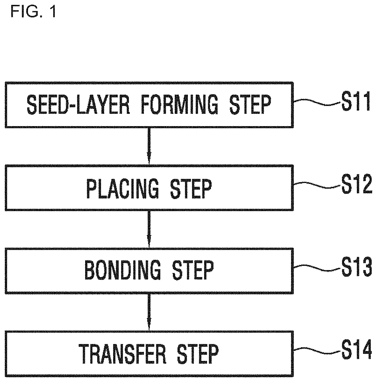
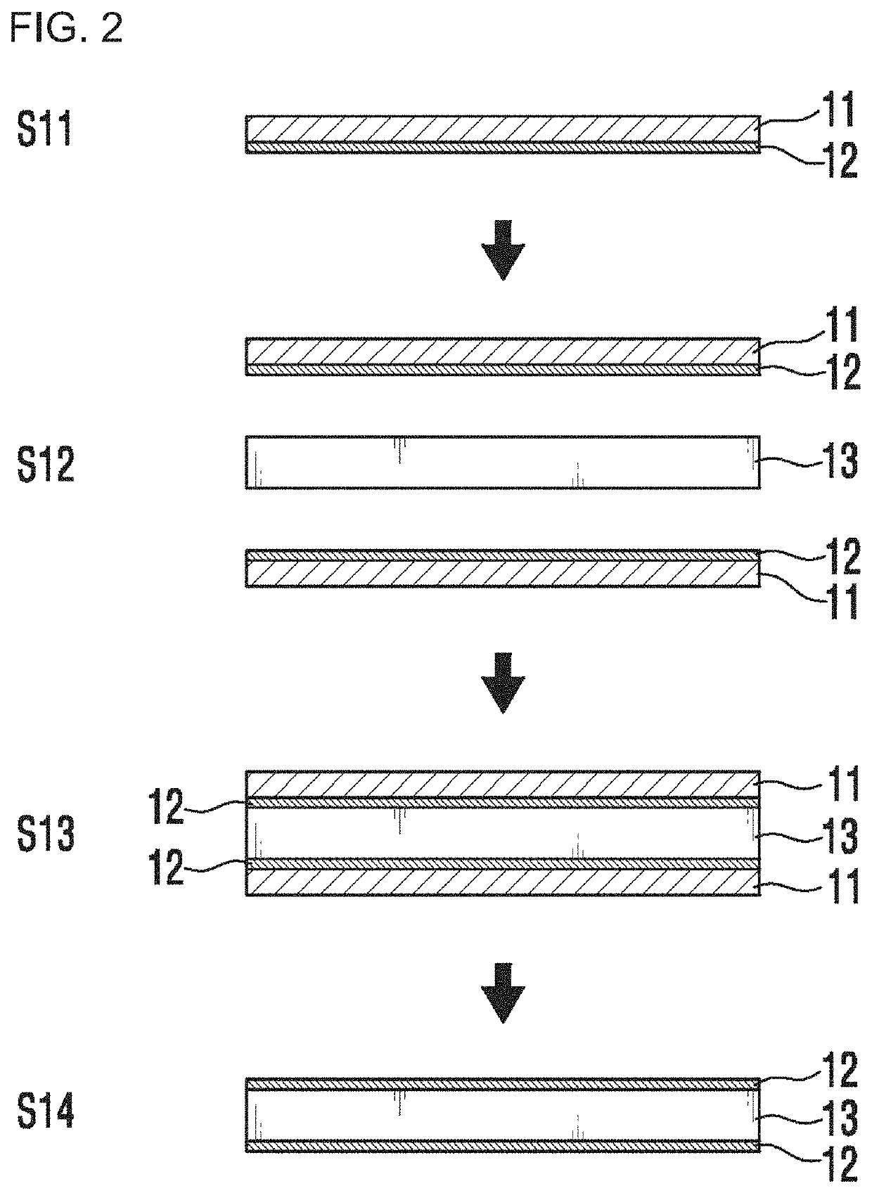
The disclosure relates to a method for manufacturing a transfer film including an electrode layer, the method comprising: an electrode layer formation step of forming an electrode layer on a carrier member by using a conductive material; a placement step of placing the carrier member on at least one side of an insulating resin layer respectively; a bonding step of bonding the carrier member and the insulating resin layer together by applying pressure thereto; and a transfer step of removing the carrier member to transfer the electrode layer on the insulating resin layer.

Description

RELATED APPLICATIONS[0001]This application is a National Phase of PCT Patent Application No. PCT / KR2018 / 002074 having International filing date of Feb. 20, 2018, which claims the benefit of priority of Korean Patent Application No. 10-2017-0022586 filed on Feb. 20, 2017. The contents of the above applications are all incorporated by reference as if fully set forth herein in their entirety.FIELD AND BACKGROUND OF THE INVENTION[0002]The present invention relates to a method of manufacturing a transfer film including a seed layer, and more particularly to a method of manufacturing a transfer film including a seed layer, in which the seed layer for forming a circuit is provided without using a copper clad film.[0003]In general, a printed circuit board refers to an electronic part given in a form of a board on which various electronic parts are mounted and electrically connected.[0004]There are various kinds of printed circuit board, such as a single-layer type, a double-sided type, a mu...

Claims


Application Information

Patent Timeline
Patent Type & Authority Patents(United States)
IPC IPC(8): C09K13/00C23F1/00C25D3/38C25D5/02H05K1/09H05K3/06H05K3/42H05K3/46C25D5/10
CPCC09K13/00C23F1/00C25D3/38C25D5/02C25D5/10H05K1/09H05K3/067H05K3/423H05K3/425H05K3/429H05K3/4652H05K2203/072H05K2203/0723H05K2203/0793H05K2203/0796H01B1/16H01B3/30H01B13/00C25D7/123C25D5/48C23C18/1653C23F1/02C23F1/44C23F1/40H05K3/108H05K3/4644H01B13/0026
Inventor CHUNG, KWANG-CHOONMOON, BYUNG WOONGKIM, SU HANKIM, JAE RIN
Owner INKTEC CO LTD
Why Eureka
Try Eureka