Semiconductor device

a semiconductor and device technology, applied in the direction of lasers, radiation controlled devices, semiconductor lasers, etc., can solve the problems of significant failure of stability damage to controllability in a manufacturing process, and the size of the substrate, so as to achieve excellent crystallinity and restrict the bowing of the substrate

Inactive Publication Date: 2001-11-01
SONY CORP
View PDF0 Cites 21 Cited by
  • Summary
  • Abstract
  • Description
  • Claims
  • Application Information

AI Technical Summary

Benefits of technology

0012] In a semiconductor device according to the present invention, the semiconductor layer having a lateral growth region is equal to or

Problems solved by technology

The bowing of the substrate causes fractures in the sapphire substrate and the bowing of the semiconductor layer of the III-V group compound of the nitride system, which fails in stability in a manufacturing process significantly.
In addition, temperature of the substrate when growing the semiconductor of the III-V group compound of the nitride system becomes unstable, and then a composition of the semiconductor of the III-V group compound of the nitride system grown thereon becomes heterogeneous depending ranges, which consequently giv

Method used


Image

  • Semiconductor device
  • Semiconductor device
  • Semiconductor device

Examples


examples 1-5

; Evaluation of the GaN Layer

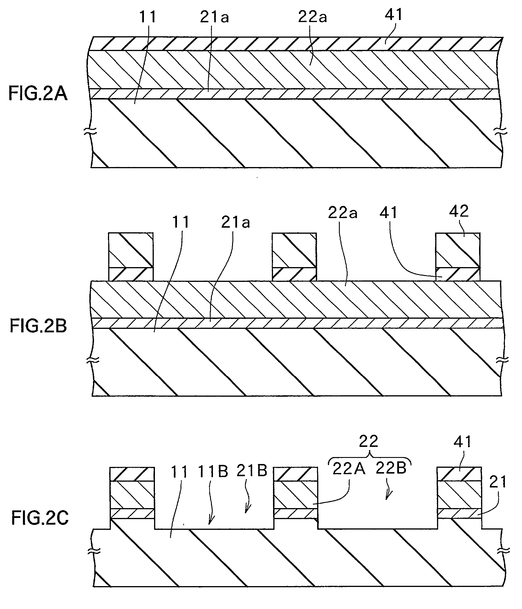
[0079] First, a substrate made of sapphire was prepared. GaN was grown on a c face of the substrate 40 nm with a MOCVD method to form a growth layer for a buffer layer. Following this, with the same MOCVD method, GaN was grown 2 .mu.m to form a growth layer for a seed crystal layer, and then, a insulating film made of silicon nitride was formed on the growth layer for a seed crystal layer with a CVD method.

[0080] Next, a photoresist film was formed on the insulating film and at the same time, a plurality of patterns with a striped shape was formed. RIE was carried out with the pattern-formed photoresist film as a mask to remove the insulating film selectively. After this, the photoresist film was removed.

[0081] After removing the photoresist film, RIE was carried out with the insulating film as a mask to remove part, which the growth layer for the seed crystal layer, the growth layer for a buffer layer, and the substrate were uncovered with the insulatin...

example 2

; Evaluation of the Semiconductor Laser Diode

[0089] Further, with the MOCVD method, a n-type clad layer, a n-type guide layer, an active layer, a p-type guide layer, a p-type clad layer and a p-side contact layer were formed onto the GaN layer of Example 2 sequentialy. Specifically, an n-type Al.sub.0.08Ga.sub.0.92N mixed crystal doped silicon was grown 1.2 .mu.m to form the n-type clad layer and n-type GaN doped silicon is grown 0.1 .mu.m to form the n-type guide layer. The active layer was formed as described hereinafter. First, an N-type GaInN mixed crystal doped silicon is grown 7.0 nm to form the barrier layer, then, an undope-GaInN mixed crystal was grown 3.5 nm to form a well layer. Finally, the active layer was formed by stacking those layers in 3 periods. P-type GaN doped magnesium was grown 0.1 .mu.m to form the p-type guide layer. A p-type Al.sub.0.08Ga.sub.0.92N mixed crystal was grown in 0.5 .mu.m to form the p-type clad layer. P-type GaN doped magnesium was grown 0.1 ....

first embodiment

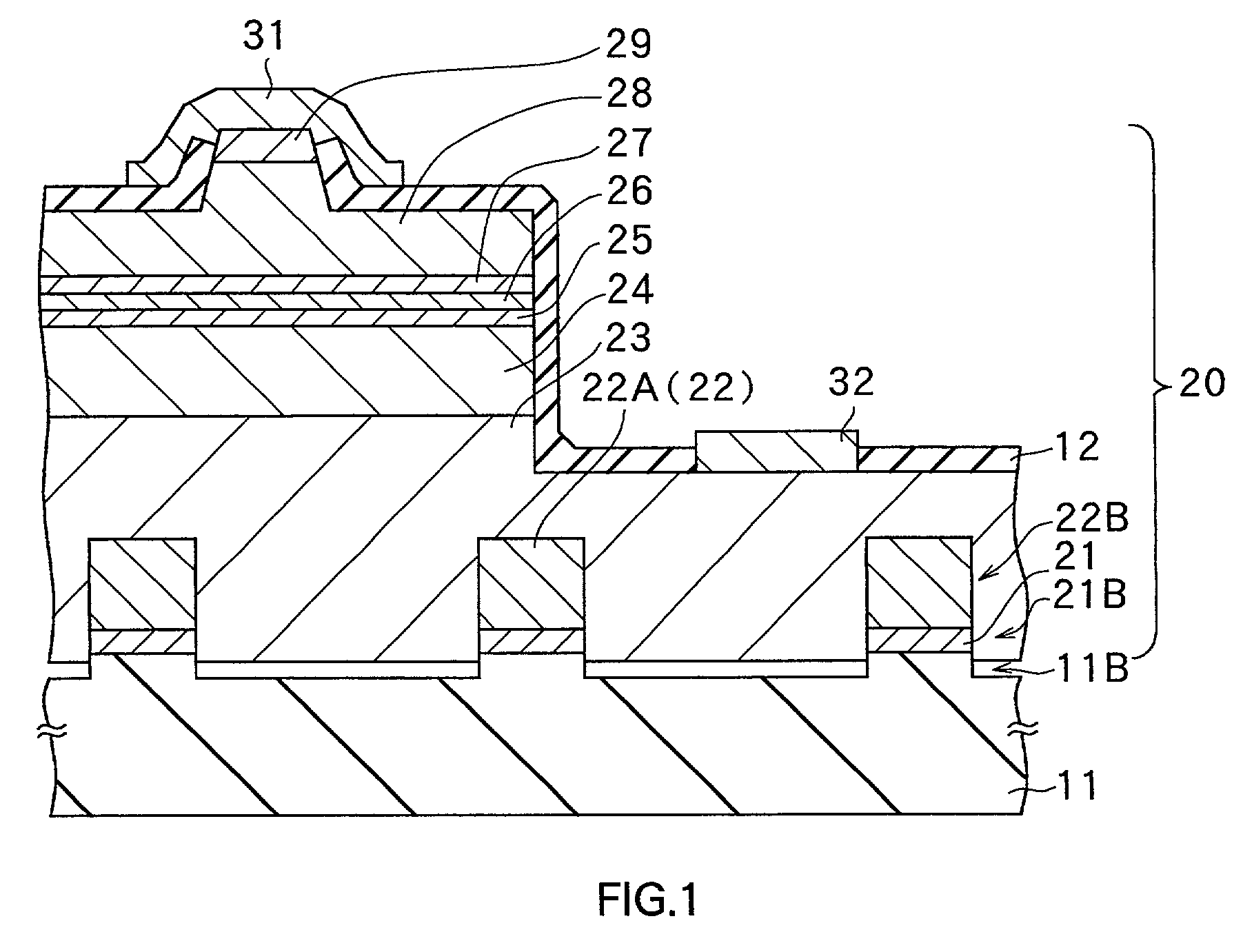
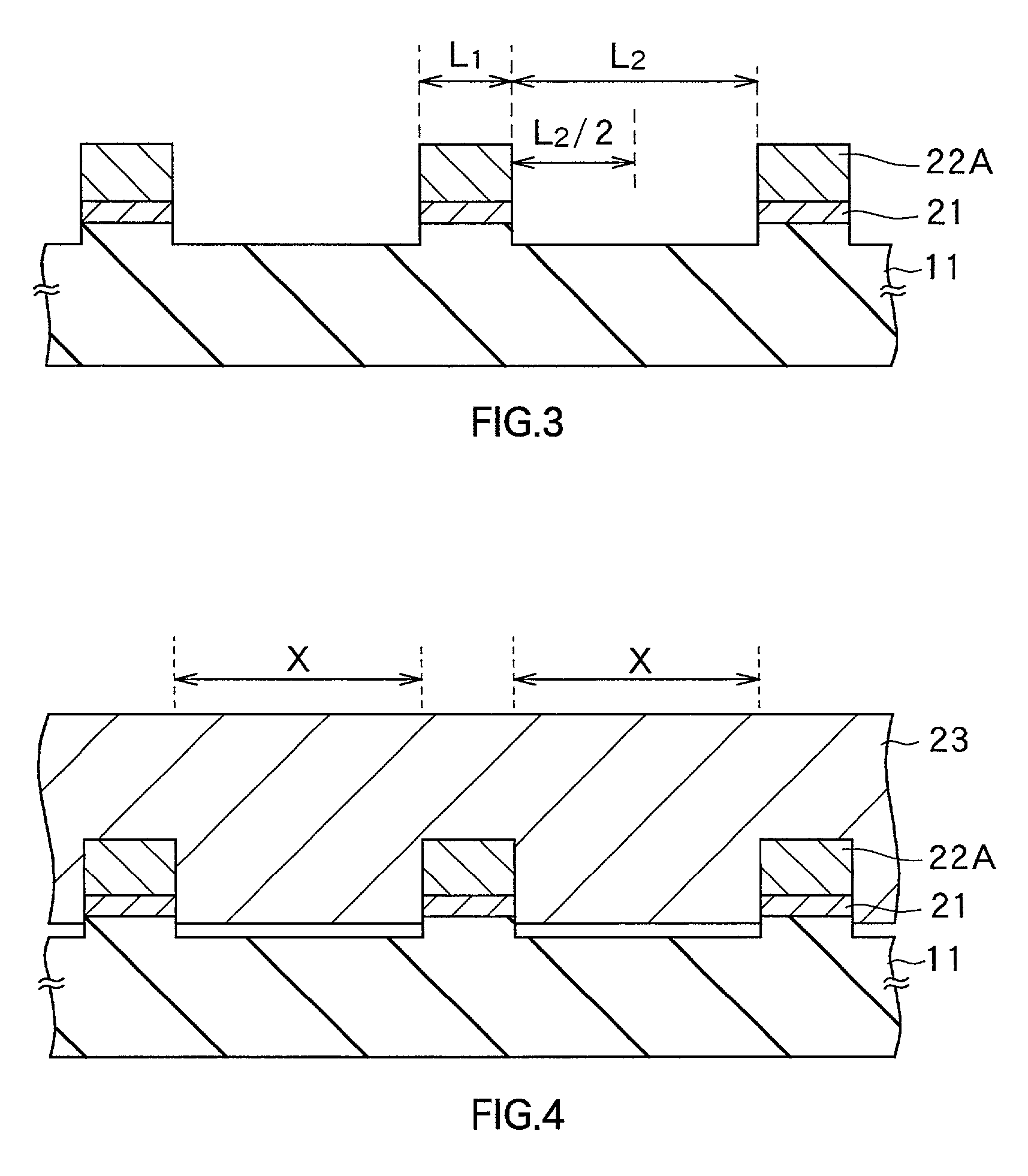
[0098] Moreover, in the above-mentioned first embodiment, after removing the insulating 41, the n-side contact layer 23 was formed. As shown in FIG. 11, the n-side contact layer 23 may be formed without removing the insulating layer 41 on the seed crystal layer 22. This shields the penetration dislocation M.sub.1 with the insulating film 41, which prevents propagation of the penetration dislocation M.sub.1 from the seed crystal layer 22. Accordingly, in the n-type contact layer 23, crystal defects hardly exist except the penetration dislocation M.sub.2, which is a cause of a meet. This can gain the semiconductor layer of the III-V group compound of the nitride system with excellent crystallinity. However, preferably, a manufacturing method may be chosen depending on a purpose for use because when growing the n-side contact layer 23, a materials contained the insulating film 41 is mixed into the n-side contact layer 23 as an impurity, which degrades characteristics of a semiconductor...


PUM


Abstract

To provide a semiconductor device capable of preventing the bowing of the substrate, and having a semiconductor layer of a III-V group compound of a nitride system with excellent crystallinity. The semiconductor layer of the III-V group compound of the nitride system whose thickness is equal to or less than 8 mum, is provided onto a substrate made of sapphire. This reduces the bowing of the substrate due to differences in a thermal expansion coefficient and a lattice constant between the substrate and the semiconductor layer of the III-V group compound of the nitride system. An n-side contact layer forming the semiconductor layer of the III-V group of the nitride system has partially a lateral growth region made by growing in a lateral direction from a crystalline part of a seed crystal layer. In the lateral growth region, dislocation density restricts low, therefore, regions corresponding to the lateral growth region of each layer formed onto the n-side contact layer has excellent crystallinity.

Description

[0001] 1. Field of the Invention[0002] The present invention relates to a semiconductor device including a semiconductor layer made of a semiconductor of a III-V group compound of a nitride system.[0003] 2. Description of the Related Art[0004] The semiconductor of the III-V group compound of the nitride system such as a GaN mixed crystal, a AlGaN mixed crystal or a GaInN mixed crystal is a direct transition semiconductor material, and at the same time, has a characteristic in such that its forbidden band width spreads from 1.9 eV to 6.2 eV. For this reason, these semiconductors of the III-V group compound of the nitride system can obtain light emission from a visible range to an ultra violet range, therefore, it is noteworthy for a material making a semiconductor light-emitting device such as a semiconductor laser diode (LD) or a laser emitting diode (LED). In connection with this, the semiconductor of the III-V group compound of the nitride system is focused attention as a material...

Claims


Application Information

Patent Timeline
IPC IPC(8): H01L21/20H01L33/06H01L33/32H01S5/323
CPCH01L33/007H01S5/32341H01S2304/12H01L21/02378H01L21/0265H01L21/02422H01L21/0254H01L21/02576H01L21/0262H01L21/0242H01L21/20
Inventor TAKEYA, MOTONOBUYANASHIMA, KATSUNORIIKEDA, MASAOASANO, TAKEHARUIKEDA, SHINROHINO, TOMONORISHIBUYA, KATSUYOSHI
Owner SONY CORP
Why Eureka
Try Eureka