
Eureka
For R&D, Eureka makes reading and utilizing patents & technical documents easy.
Eureka AIR
Designed for self-driven R&D workflows. Generate viable solutions, solve complex R&D challenges, empower your innovation with AI.

Eureka Materials
Designed for material experts only. Revolutionize your material R&D, from search, analyze, to developing new materials.

TechResearch
Generate reliable direction feasibility study reports for your R&D in just a few steps.

TechSeek
Discover and master advanced knowledge NOW. Basics, ideas, possibilities, all at once.

TechMind
As an expert in R&D Theories, TechMind can generates customized viable solutions instantly.

TechRisk
Analyze your overall solution with one click, know your potential R&D risks in advance.

TechMonitor
Get weekly tech updates, stay abreast of the latest tech innovations and key insights.
Solar cell device
- Summary
- Abstract
- Description
- Claims
- Application Information
AI Technical Summary
Problems solved by technology
Method used
Image

Examples
first embodiment
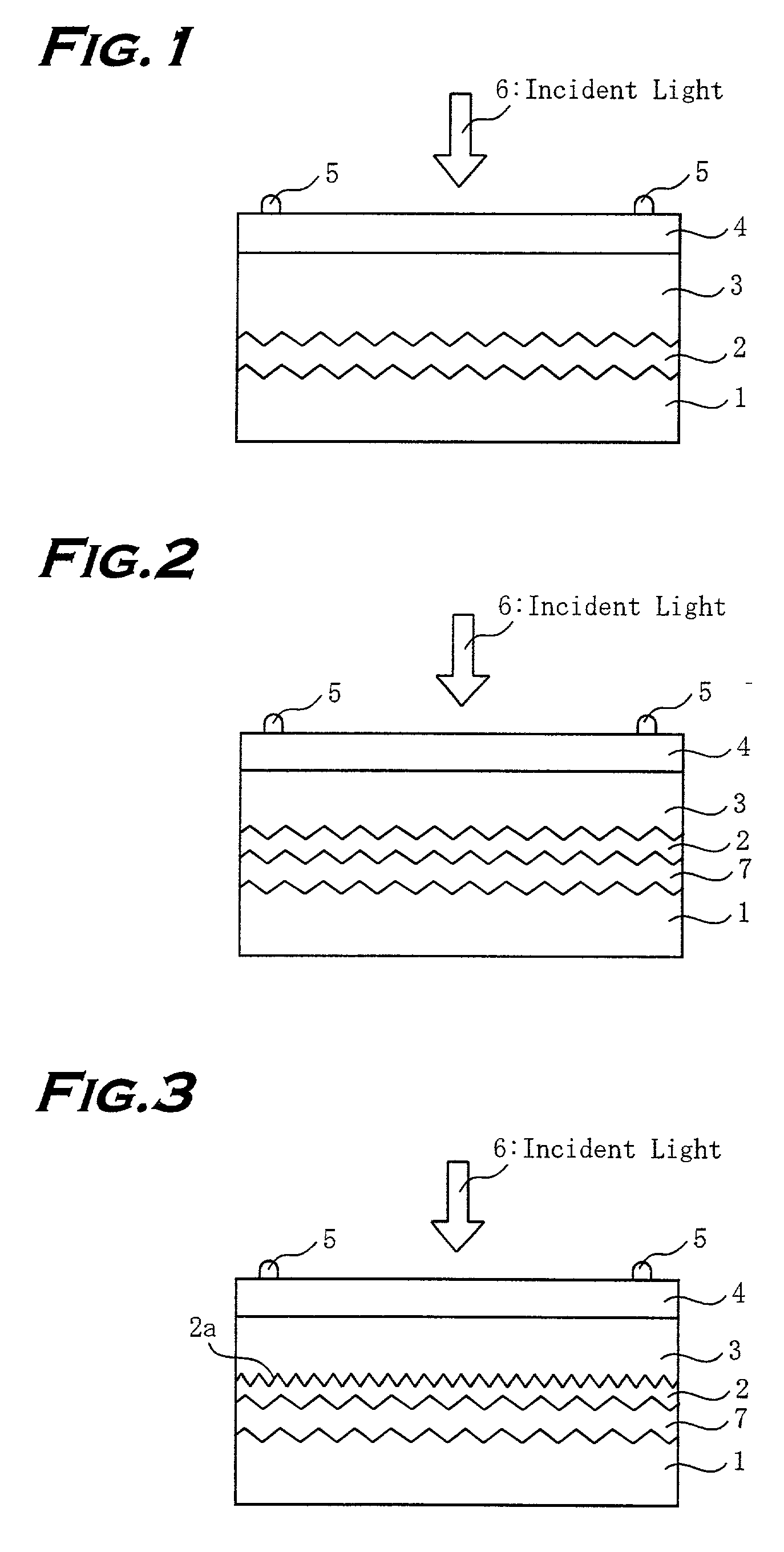
[0029] FIG. 1 is a cross sectional view illustrating a structure of a thin film solar cell device of the invention. A substrate 1 is a metal foil of copper, nickel, iron or the like of 10-500 .mu.m in thickness produced by electroforming or a metal foil of alloy of these material. The substrate 1 used in this embodiment is an electroformed copper foil.
[0030] "Wet processing handbook" (FOUNDATION ADVANCED TECHNOLOGY INSTITUTE, published on Mar. 22, 1996, 108-123 pages) describes on electroforming, for example. In general, a drum is dipped in an electrolyte bath, metal is deposited on the drum to be thick, and then the electrically deposited material is peeled from the drum to produce into product or duplicate. In manufacturing a copper foil by electroforming, copper electrolyte used in electroforming is acid copper-sulfate containing copper-sulfate of 200 g / l. A drum of titan, stainless steel or the like is partially dipped in the electrolyte bath filled with the acid copper-sulfate,...
second embodiment
[0041] The metal layer of high optical reflectivity of the second embodiment is formed by coating silver (Ag) of 3000 .ANG. in thickness on the rough metal foil substrate 1 by radio frequency (RF) sputtering. The silver is formed under the conditions of argon (Ar) gas atmosphere, reaction pressure of 0.399 Pa, radio frequency power density of 3 W / cm.sup.2, a substrate temperature of room temperature.
[0042] Then a transparent conductive material layer 2 of such as tin oxide, indium tin oxide, and zinc oxide is coated on the metal layer 7 by sputtering.
[0043] Then, a photovoltaic conversion layer 3 of a thin film semiconductor layer mainly containing amorphous silicon or the like is formed on the transparent conductive material layer 2. As like in the first embodiment, an n-type layer of amorphous silicon layer of 200 .ANG., an i-type layer of amorphous silicon layer of 3000 .ANG., a p-type layer of amorphous silicon carbide layer of 100 .ANG. are laminated in this order from the roug...
third embodiment
[0055] The transparent conductive material layer 2 of the third embodiment is wet-etched by 0.1-2% hydrochloric acid after forming a zinc oxide layer of approximately 0.7-1 .mu.m. The wet-etching can be conducted by using acetic acid aqueous solution other than hydrochloric acid and dipping the layer in it for 10-60 seconds at a room temperature. The rough shape 2a of the transparent conductive material layer 2 can also be formed by dry etching and ion etching.
[0056] The transparent conductive material layer 2 of such as tin oxide, indium tin oxide, and zinc oxide having a fine rough shape formed on the metal foil substrate 1 enables to utilize incident light such as sunlight so as to improve efficiency of the solar cell.
[0057] Then, characteristics of the thin film solar cells of the first-third embodiments and a thin film solar cell of a conventional structure are compared. For the thin film solar cell of the conventional structure, a substrate of a glass coated with tin oxide (Sn...
PUM
 Abstract
Description
Claims
Application Information
 - R&D Engineer
- R&D Manager
- IP Professional
- Industry Leading Data Capabilities
- Powerful AI technology
- Patent DNA Extraction
Browse by: Latest US Patents, China's latest patents, Technical Efficacy Thesaurus, Application Domain, Technology Topic, Popular Technical Reports.
© 2024 PatSnap. All rights reserved.Legal|Privacy policy|Modern Slavery Act Transparency Statement|Sitemap|About US| Contact US: help@patsnap.com