
Delay circuit, voltage-controlled delay circuit, voltage-controlled oscillation circuit, delay adjustment circuit, DLL circuit, and PLL circuit

a delay circuit and voltage control technology, applied in the field of delay circuits, can solve the problems of increased susceptibility to process variations, reduced pull-in speed, and difficulty in designing a pll circuit of a very high multiplication factor

Inactive Publication Date: 2002-03-21
SONY CORP
View PDF0 Cites 27 Cited by
  • Summary
  • Abstract
  • Description
  • Claims
  • Application Information

AI Technical Summary

Problems solved by technology

A delay time of a delay circuit or a voltage-controlled delay circuit changes when there is a power source noise, such as changes of a power source voltage.
Therefore, it is very difficult to design a PLL circuit of a very high multiplication factor wherein the multiplication factor is several thousand to ten thousand times.
PLL circuits have been designed by solving characteristic formulas of feedback loops, so the techniques for reducing jitter of a PLL or DLL have mainly focused on techniques for achieving both high speed pull-in and reduced jitter (making filter characteristics variable etc.) It is considered better to reduce the gain of a PLL circuit by characteristic formulas to realize lower jitter, but when reducing the gain of the PLL circuit, there are problems that the pull-in speed declines and there is greater susceptibility to process variations.
However, since power source voltage dependency was not included in the characteristic formula of the feedback loop, designers of PLL circuits did not view design of a circuit having a small power source voltage dependency as being a general problem.
Therefore, the above measures did not consider the jitter caused by power source noise in a locked state--which becomes a problem in a PLL of a high multiplication factor and low jitter used for displaying a video signal on a personal computer and displaying OSD letters on a TV monitor.
Furthermore, if designed well, it has a good PSRR (power supply rejection ratio) and becomes resistant to digital noise--which becomes a problem when building the circuit into the chip.
In this way, differential circuit designers considered the design of a circuit having a small power source voltage dependency to be a general problem.
Since differential circuit does not require full swing of an input / output signal, it can operate at a high speed, but it has the disadvantage that the output amplitude is not constant and the delay time is liable to change since the signal does not fully swing.
Therefore, the power consumption and layout area become twice compared with a non-differential circuit.
However, since a clamp circuit and feedback circuit have to be attached, there are disadvantages that the power consumption is further increased and the speed does not become as high as expected.
Also, since a signal which does not fully swing has to be converted to a signal which fully swings at the time of taking out an output signal, the duty is liable to go wrong.
Further, the differential circuit has a large number of transistors connected in the vertical direction so measures have to be made to secure an operating margin when reducing the power source voltage of the semiconductor integrated circuit.
Therefore, there are many technical problems in differential PLL circuits and DLL circuits.
The power source noise generated at the time of operating an output buffer is for example a pulse noise.
When the control voltage Vcntn becomes high, the ratio of the period of driving the heavy load capacitance of Cg+Cs increases, so the delay time becomes long.
Since a load capacitance value changes in the middle in the case of a shunt-type delay stage, it is difficult to consider generally.
Also, if the impurity concentrations of both P and N on a junction face are high, care is needed because the breakdown voltage will fall and the leak current will increase in some cases.
Note that when forming a super step junction capacitor, the wafer process becomes complicated.
As a result, there is a high possibility of an increase of the cost of the semiconductor chip.
Since the buffer and logic gate as above do not receive as input a control signal and bias signal, they are affected by power source noise.
Therefore, a change of the delay time ends up occurring when there is power source noise in this part.
As the power source voltage becomes higher, the delay time becomes larger.
On the other hand, a B-type delay stages does not have any countermeasure against the power source noise and has a large power source dependency.
Since the B-type delay stage provided as the switching circuit is not controlled by a control voltage Vcntn or a bias voltage Vcntp, the delay time sometimes changes due to the effect of power source noise.
Namely, since there is no portion corresponding to S1 in the Lag filter, a large amount of the effect of digital power source noise remains as the inherently not desirable change of the control voltage, consequently the amount of jitter becomes large.
When coincidentally designed so that a change of the S1 portion unfortunately arises while a portion not related with the control voltage and bias voltage is in operation, it is considered that an effect of phase pull-in of the S1 portion is not obtained and jitter becomes large when a width of the S1 portion is small.

Method used


Image

  • Delay circuit, voltage-controlled delay circuit, voltage-controlled oscillation circuit, delay adjustment circuit, DLL circuit, and PLL circuit
  • Delay circuit, voltage-controlled delay circuit, voltage-controlled oscillation circuit, delay adjustment circuit, DLL circuit, and PLL circuit
  • Delay circuit, voltage-controlled delay circuit, voltage-controlled oscillation circuit, delay adjustment circuit, DLL circuit, and PLL circuit

Examples


second example

OF APPLICATION

[0387] FIG. 41 is a circuit diagram of an example of application of the voltage-controlled oscillation circuit (VCO) of the present invention and shows a PLL circuit configured by using the VCO of the present example.

[0388] As shown in the figure, the PLL circuit of the present example is comprised of a phase comparator 10, a charge pump circuit 20, a filter 30, a VCO 40, and a frequency divider 50.

[0389] Note that, as shown in FIG. 41, the PLL circuit of the present example of application has almost the same configuration as a conventional PLL circuit. Note that even when the phase comparator 10, charge pump circuit 20, or the filter 30 is as same as a conventional type, it is possible to obtain an effect of remarkably reducing jitter caused by the power source voltage after pull-in by the PLL circuit by using the VCO of the present invention.

[0390] Note that since the effect of the present invention is obtained when a variety of conditions are attained well, the inve...

third example

OF APPLICATION

[0398] FIG. 43 is a circuit diagram of a PLL circuit configured by using the VCO of the present invention and a dot clock generation circuit including this PLL circuit.

[0399] The dot clock generation circuit of the present example can be applied for example to a generation circuit for generating a dot clock and a VBI sampling clock for digital TV. The PLL circuit for example uses as a reference clock a horizontal synchronization signal HSYNC selected from a horizontal synchronization signal HSYNC0 of a main screen or a horizontal synchronization signal HSYNC1 of a sub-screen and synchronizes with a frequency divider output at a rising edge (corresponding to a right end of the screen) of the same. The charge pump circuit operates at the right end of the screen.

[0400] As shown in the figure, the PLL circuit portion is comprised of a phase comparator 10, charge pump 20, filter 30, VCO 40, frequency divider 50, and bias circuit 70. Other than the PLL circuit, a control cir...


PUM


Abstract

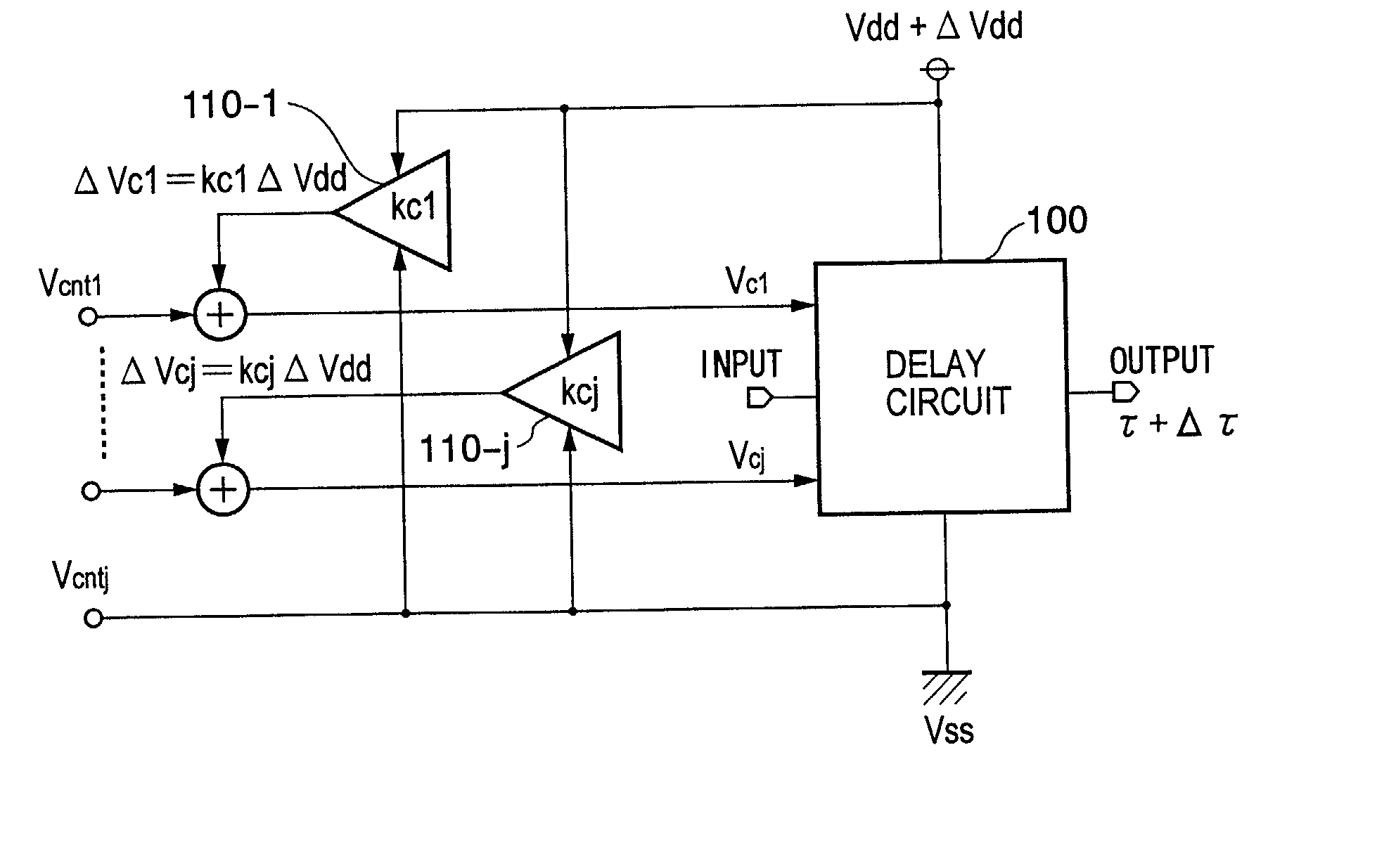
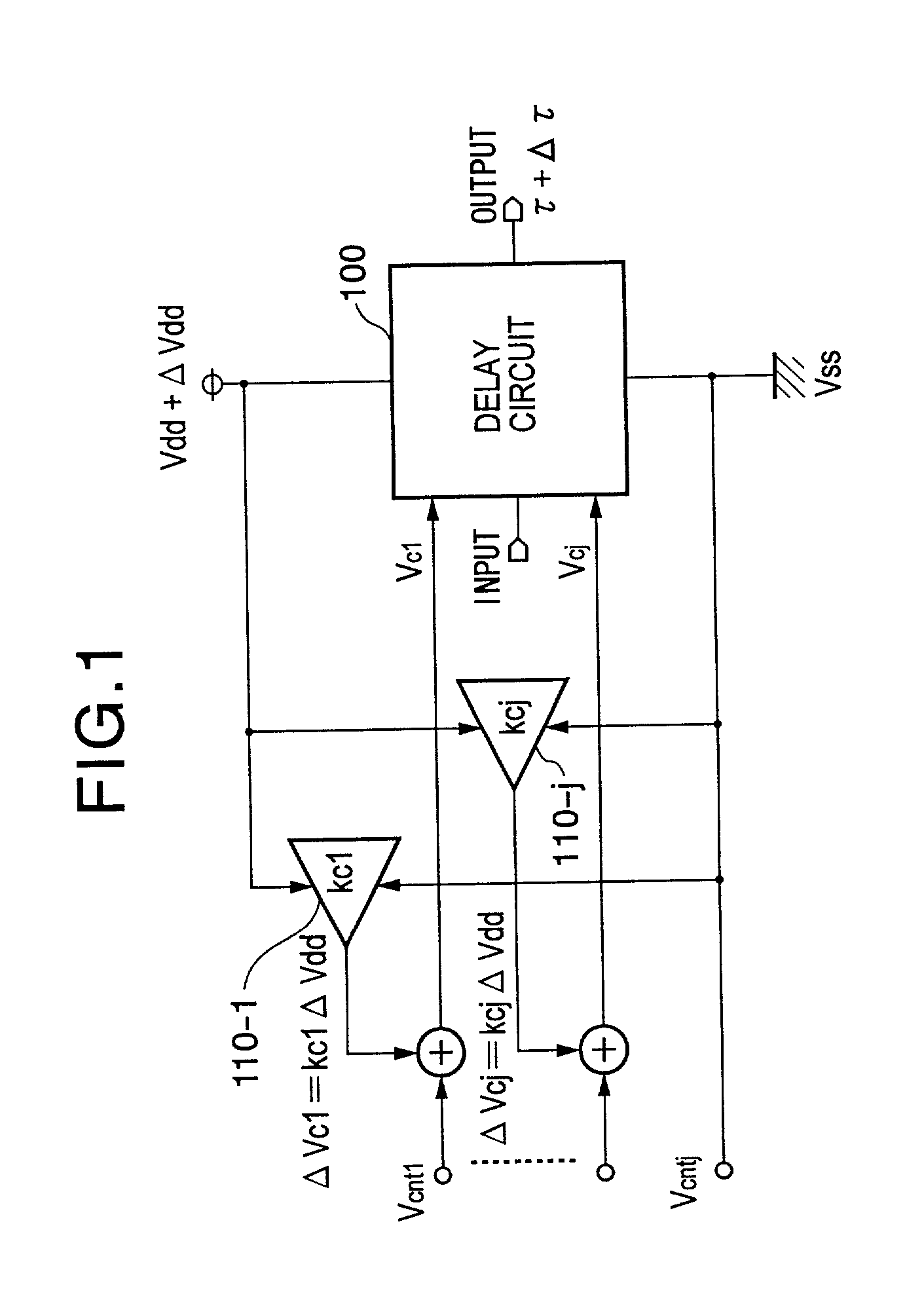
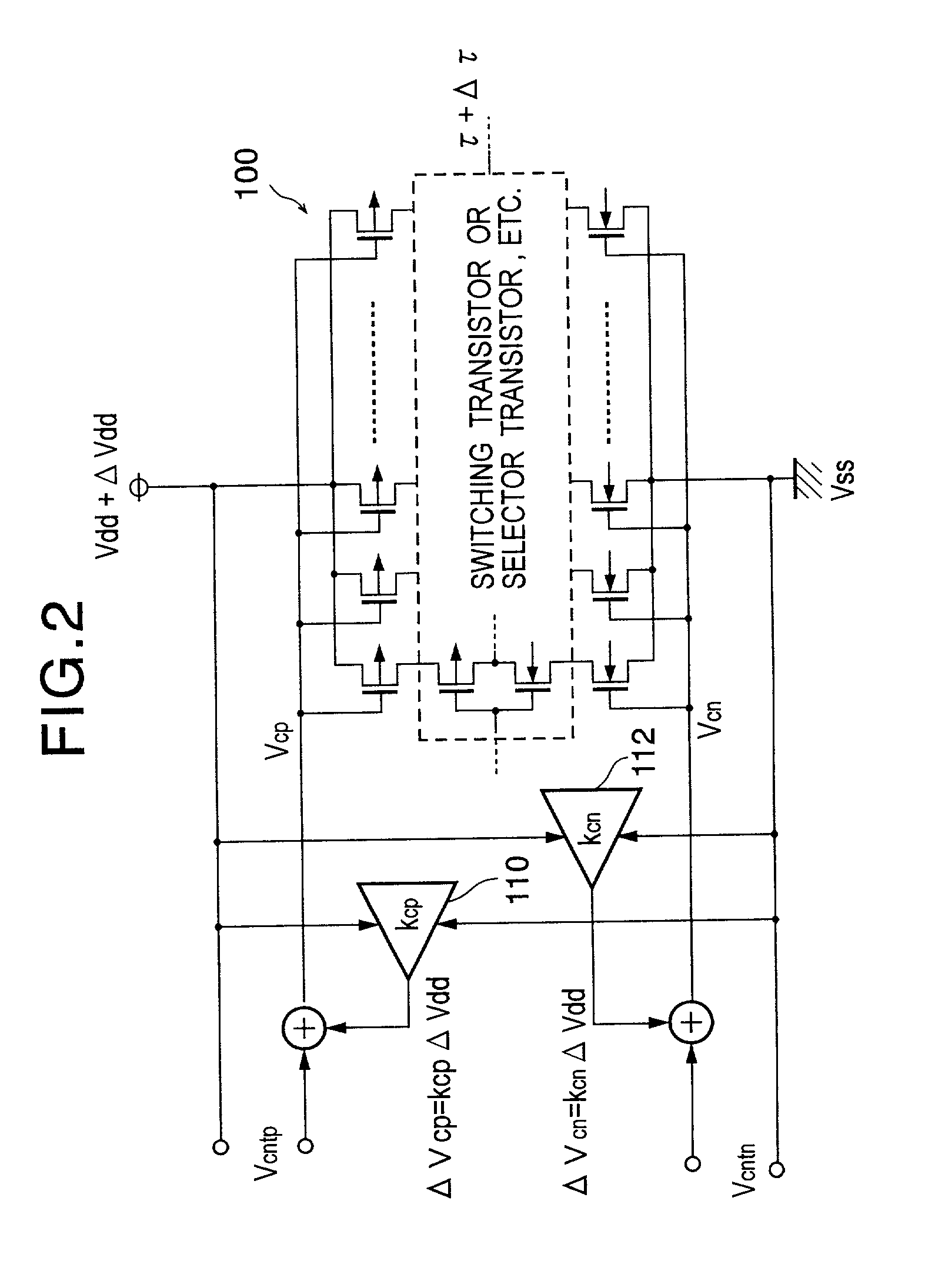
An inverter type delay circuit, voltage-controlled oscillation circuit, and voltage-controlled delay circuit capable of realizing simplification of circuit configuration, reduction of an effect of power source noise, and reduction of jitter, wherein a delay circuit, voltage-controlled oscillation circuit, and voltage-controlled delay circuit comprised of a plurality of delay stages controlled in drive current in accordance with a bias voltage or a control voltage and determined in delay time by the drive current, adding a change of a power source voltage to the above bias voltage or control voltage by a predetermined ratio and supplying a result of the addition to the above delay stages to suppress the power source voltage dependencies of the delay times of the delay stages, or connecting by a predetermined ratio a plurality of delay stages having different power source voltage dependencies, for example, power source voltage dependencies of opposite delay times, to suppress the power source voltage dependencies of delay times of the delay stages are realized.

Description

[0001] 1. Field of the Invention[0002] The present invention relates to a delay circuit, for example, a delay circuit having a stable delay time or a voltage-controlled delay circuit capable of controlling a delay time in accordance with a control voltage, furthermore, a voltage-controlled oscillation circuit capable of controlling an oscillation frequency in accordance with a control voltage, a delay adjustment circuit using a delay circuit, a DLL (Delay Locked Loop) circuit, and a PLL (Phase Locked loop) circuit.[0003] 2. Description of the Related Art[0004] A delay time of a delay circuit or a voltage-controlled delay circuit changes when there is a power source noise, such as changes of a power source voltage. Further, in an oscillation circuit configured by a plurality of delay circuits connected in a ring, it is possible to configure a voltage-controlled oscillation circuit (VCO) by controlling the delay times of the delay circuits in accordance with control voltages. When pow...

Claims


Application Information

Patent Timeline
IPC IPC(8): H03H11/26H03K3/013H03K3/03H03K3/354H03K5/00H03K5/13H03L7/081H03L7/089H03L7/099
CPCH03K3/013H03K3/0315H03K5/133H03K2005/00039H03K2005/00065H03K2005/00071H03K2005/00195H03K2005/00202H03L7/0812H03L7/0893H03L7/0995H03L7/0816H03L7/099
Inventor TACHIMORI, HIROSHI
Owner SONY CORP
Learn More