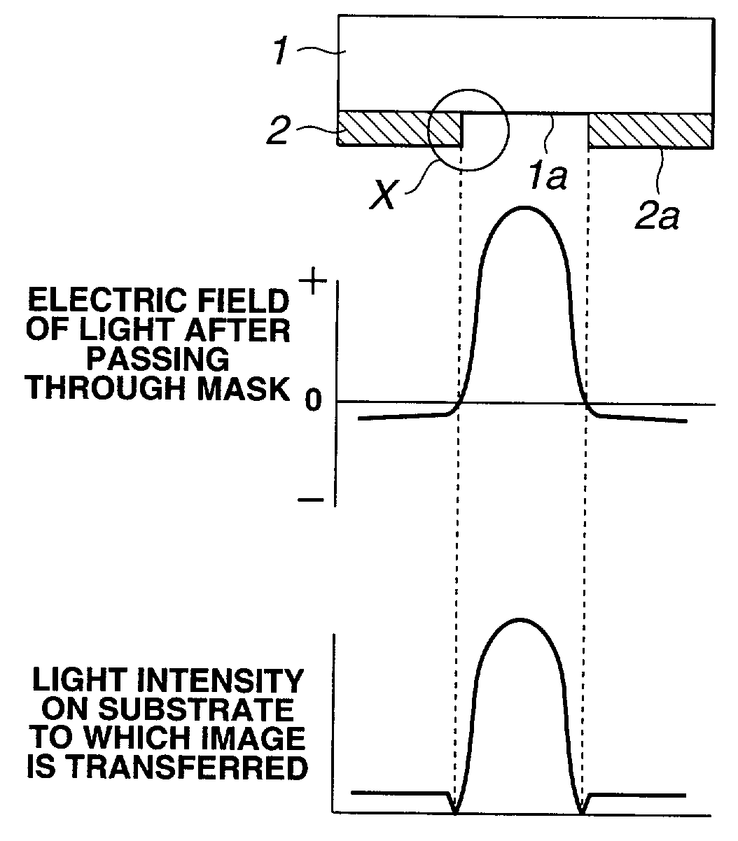
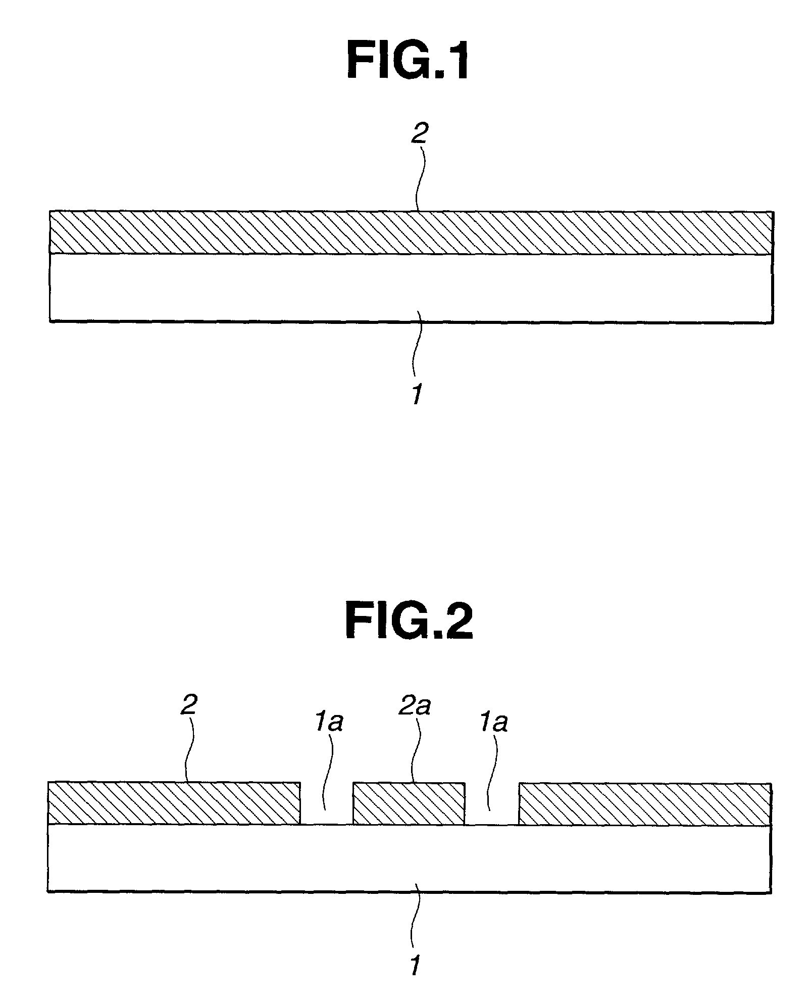
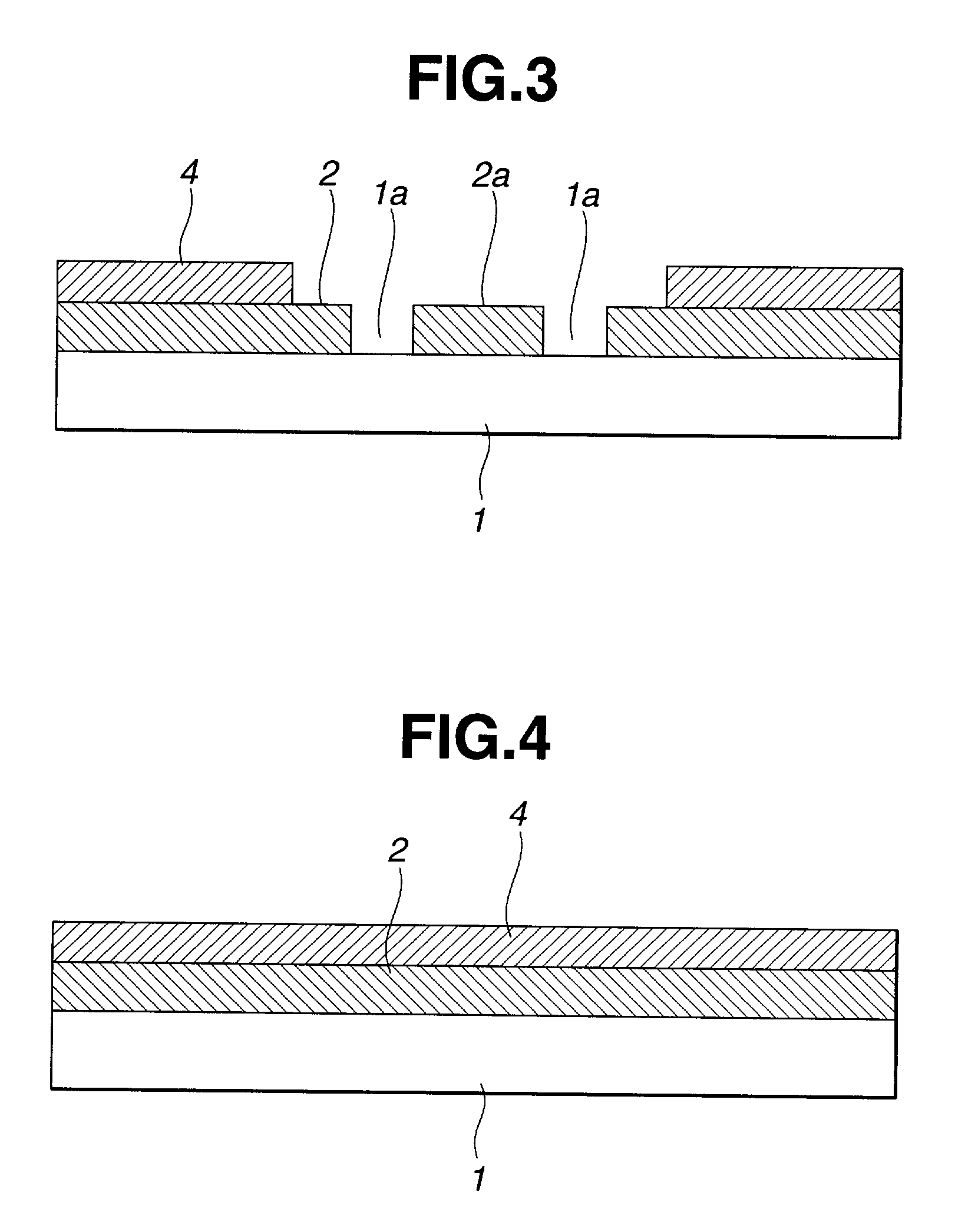
Phase shift mask blank, phase shift mask, and methods of manufacture

a technology of phase shift mask and blank, applied in the field of phase shift mask blank and phase shift mask, can solve the problems of reducing the focal depth, affecting the product yield, and lowering the process stability

Inactive Publication Date: 2002-04-04
SHIN ETSU CHEM IND CO LTD
View PDF0 Cites 5 Cited by
  • Summary
  • Abstract
  • Description
  • Claims
  • Application Information

AI Technical Summary

Problems solved by technology

However, while exposure using shorter wavelength light does improve resolution, it also has a number of undesirable effects, such as reducing the focal depth, lowering process stability and adversely impacting product yield.
In the above-described phase shift mask blanks and phase shift masks, if the phase shift film has a larger film stress than necessary, this may cause an originally flat substrate to warp after formation of the phase shift film, resulting in a loss of flatness in the phase shift mask blank.
However, the degree of film stress released by patterning is strongly affected by the pattern density and shape, and cannot be strictly determined.
Thus, no matter how carefully the amount of warp is predicted, obtaining a flat phase shift mask is very difficult.
When a phase shift mask blank having such a high-stress phase shift film and a phase shift mask obtained by patterning such a blank are actually used to transfer a circuit pattern, warping of the mask causes it to deviate from the intended position designed for it within the exposure system, which results in shifting of the focal point.
The optimal exposure conditions thus differ from region to region on the mask and focal shifts occur even within the plane of the exposure pattern, giving rise to non-uniformity in the plane of the pattern.
The result is a poor exposure margin.
It is thus difficult to stably manufacture phase shift masks of a high in-plane uniformity that are suitable for use in exposure processes.
However, altering the film forming conditions is not a desirable course of action because the optical properties of the phase shift film are strongly affected by the film forming conditions.

Method used


Image

  • Phase shift mask blank, phase shift mask, and methods of manufacture
  • Phase shift mask blank, phase shift mask, and methods of manufacture
  • Phase shift mask blank, phase shift mask, and methods of manufacture

Examples


example 1

[0047] A MoSiONC film was formed on a quartz substrate to a thickness of 140 nm by carrying out reactive sputtering in a sputtering system using molybdenum silicide as the sputtering target and using a mixture of argon, carbon dioxide and nitrogen as the sputtering gas.

[0048] The optical properties for 248 nm light, specifically the phase shift difference and transmittance, of the resulting sample were measured. The phase shift film was found to provide a phase shift of 182 degrees and a transmittance of 8.3%. The composition of this sample film, as determined by x-ray photoelectron spectroscopy (XPS), was 14 atom % molybdenum, 23 atom % silicon, 46 atom % oxygen, 10 atom % nitrogen, and 8 atom % carbon.

[0049] The change in flatness following formation of the MoSiONC film, relative to before film formation, within a 144.times.144 mm square on the 152.times.152.times.6.35 mm substrate obtained, was measured with an FT-900 flatness tester (manufactured by Nidek Co., Ltd.). The value w...


PUM

PropertyMeasurementUnit
transmittanceaaaaaaaaaa
thicknessaaaaaaaaaa
transmittanceaaaaaaaaaa

Abstract

A phase shift mask blank includes a transparent substrate and a phase shift film thereon. The phase shift film is composed primarily of a metal and silicon, typically molybdenum silicide oxide carbide or molybdenum silicide oxide nitride carbide, and has a film stress no higher than 100 MPa. The low stress makes it possible to maintain a good substrate flatness when the phase shift film is formed during production of the phase shift mask blank, and when the phase shift film is patterned during production of a phase shift mask from the blank.

Description

[0001] 1. Field of the Invention[0002] The present invention relates to phase shift mask blanks and phase shift masks suitable for use in photolithography associated with the microfabrication of electronic products such as semiconductor integrated circuits, charge-coupled devices, color filters for liquid-crystal displays, and magnetic heads. The invention relates also to methods of manufacturing such phase shift mask blanks and phase shift masks.[0003] The invention relates most particularly to halftone phase shift mask blanks and phase shift masks which can attenuate the intensity of exposure wavelength light with a phase shift film, and to methods of manufacturing such phase shift mask blanks and phase shift masks.[0004] 2. Prior Art[0005] The photomasks that are used in a broad range of applications, including the manufacture of semiconductor integrated circuit (IC) and large-scale integration (LSI) chips, are basically composed of a transparent substrate on which a light-shield...

Claims


Application Information

Patent Timeline
Patent Type & Authority Applications(United States)
IPC IPC(8): C23C14/06G03F1/32G03F1/68
CPCG03F1/0084G03F1/08G03F1/34G03F1/32G03F1/26
Inventor INAZUKI, YUKIOMURUYAMA, TAMOTSUKANEKO, HIDEOOKAZAKI, SATOSHI
Owner SHIN ETSU CHEM IND CO LTD
Why Eureka
Try Eureka