

Light emitting device, electronic equipment, and method of manufacturing thereof
a technology of light emitting devices and electronic equipment, which is applied in the direction of discharge tubes/lamp details, discharge tubes luminescnet screens, electric discharge lamps, etc., can solve the problems of degrading the device by heat, light, moisture, and oxygen easily reaching
- Summary
- Abstract
- Description
- Claims
- Application Information
AI Technical Summary
Benefits of technology
Problems solved by technology
Method used
Image

Examples
embodiment 1
[0068] [Embodiment 1]
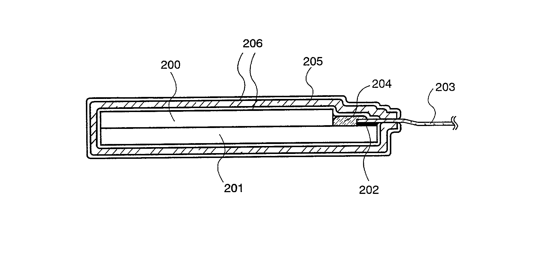
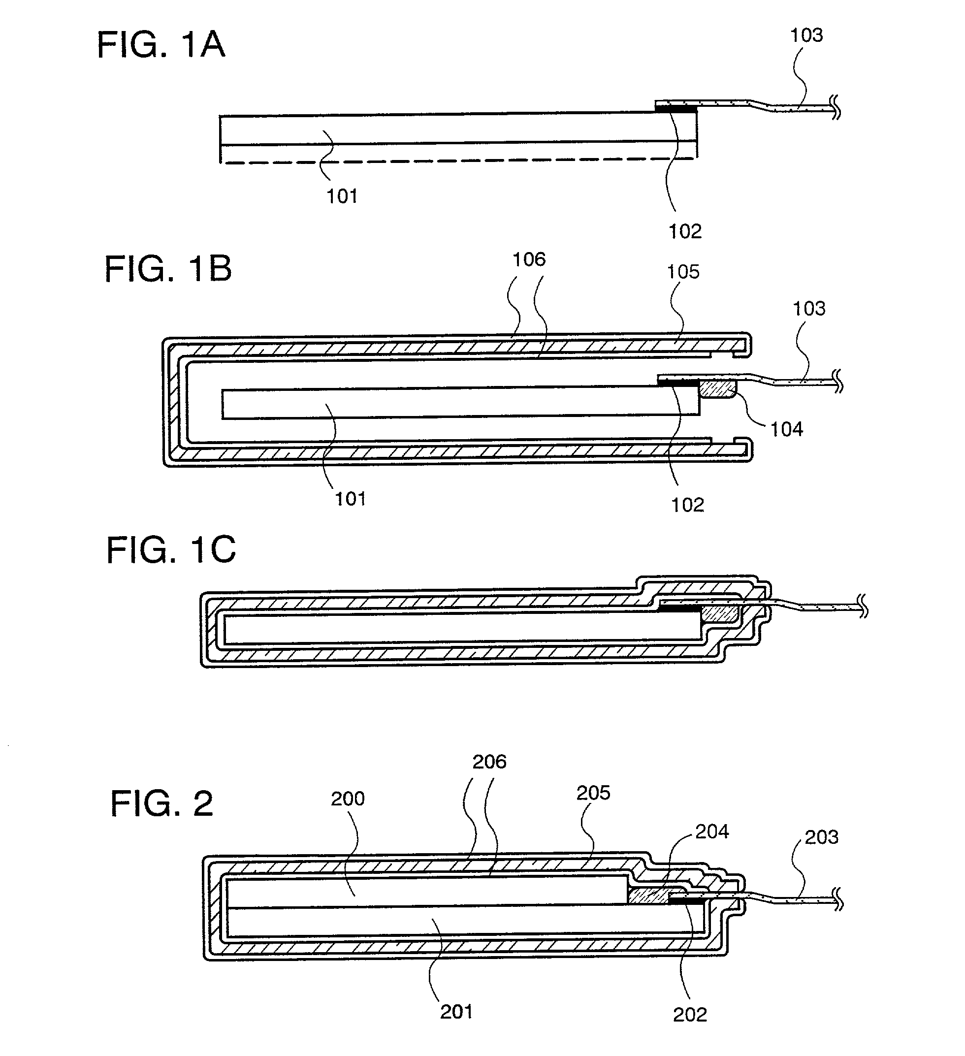
[0069] FIG. 4A is a top view of an OLED module manufactured. FIG. 4B is a sectional view schematically showing one pixel of the module of FIG. 4A.
[0070] A pixel portion 404 is arranged on a substrate 401 such that a source line driving circuit 402 and a gate line driving circuit 403 respectively run parallel to two sides of the pixel portion. The pixel portion 404, the source line driving circuit 402, and the gate line driving circuit 403 each have a plurality of TFTs. FIG. 4B shows, as representatives of those TFTs, a driving circuit TFT (composed of an n-channel TFT and a p-channel TFT in FIG. 4B) 411 included in the source line driving circuit 402 and a driving TFT (a TFT for controlling a current flowing into the OLED) 412 included in the pixel portion 404. The TFTs 411 and 412 are formed on a base film 410.
[0071] In this embodiment, the n-channel TFT and the p-channel TFT that constitute the driving circuit TFT 411 are manufactured by a known method, and a ...
embodiment 2
[0082] [Embodiment 2]
[0083] Next, described with reference to FIGS. 5 to 7 is an example of a method of manufacturing a substrate (active matrix substrate) using the light-emitting device of the present invention. Here, the method of simultaneously forming, on the same substrate, the switching TFT and the driving TFT of the pixel portion, and the TFTs of a driving portion provided surrounding the pixel portion is described in detail according to steps.
[0084] This embodiment uses a substrate 500 of a glass such as barium borosilicate glass or aluminoborosilicate glass as represented by the glass #7059 or the glass #1737 of Corning Co. There is no limitation on the substrate 500 provided it has a property of transmitting light, and there may be used a quartz substrate. There may be further used a plastic substrate having heat resistance capable of withstanding the treatment temperature of this embodiment.
[0085] Referring next to FIG. 5A, a base film 501 comprising an insulating film s...
embodiment 3
[0122] [Embodiment 3]
[0123] The light-emitting device is of the self-emission type, and thus exhibits more excellent recognizability of the displayed image in a light place as compared to the liquid crystal display device. Furthermore, the light-emitting device has a wider viewing angle. Accordingly, the light-emitting device can be applied to a display portion in various electronic devices.
[0124] Such electronic devices using a light-emitting device of the present invention include a video camera, a digital camera, a goggles-type display (head mount display), a navigation system, a sound reproduction device (a car audio equipment and an audio set), note-size personal computer, a game machine, a portable information terminal (a mobile computer, a portable telephone, a portable game machine, an electronic book, or the like), an image reproduction apparatus including a recording medium (more specifically, an apparatus which can reproduce a recording medium such as a digital video disc...
PUM
 Abstract
Description
Claims
Application Information