

Semiconductor device and method of manufacturing the same
a technology of semiconductor devices and semiconductor films, applied in semiconductor devices, semiconductor/solid-state device details, electrical equipment, etc., can solve problems such as difficulty in forming copper films, difficulty close to being solved, and apparatus problems such as shallow penetration
- Summary
- Abstract
- Description
- Claims
- Application Information
AI Technical Summary
Benefits of technology
Problems solved by technology
Method used
Image

Examples
embodiment 1
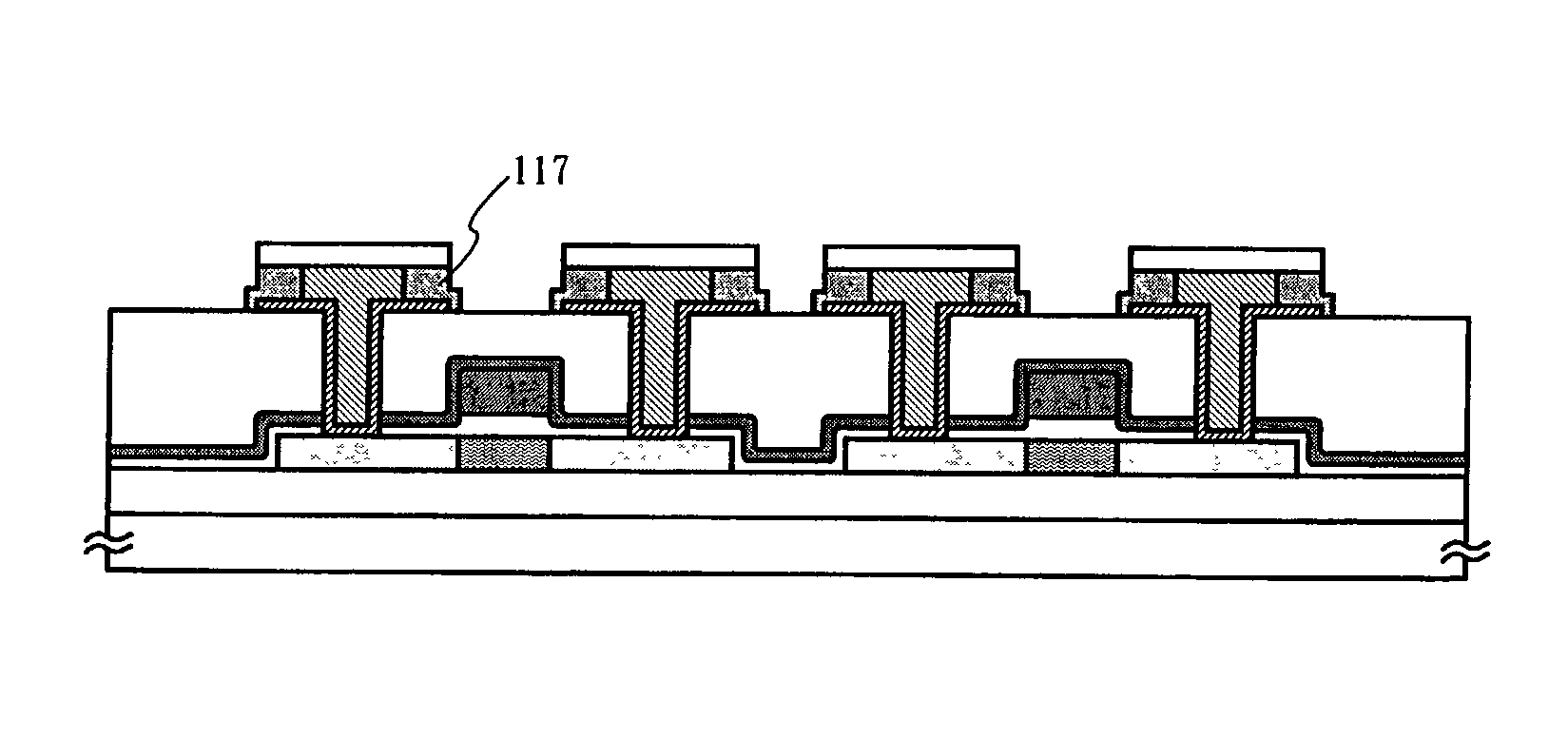
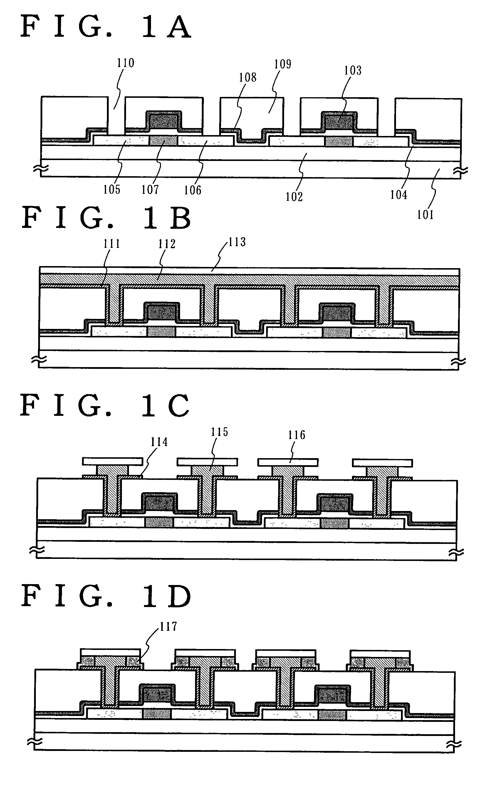
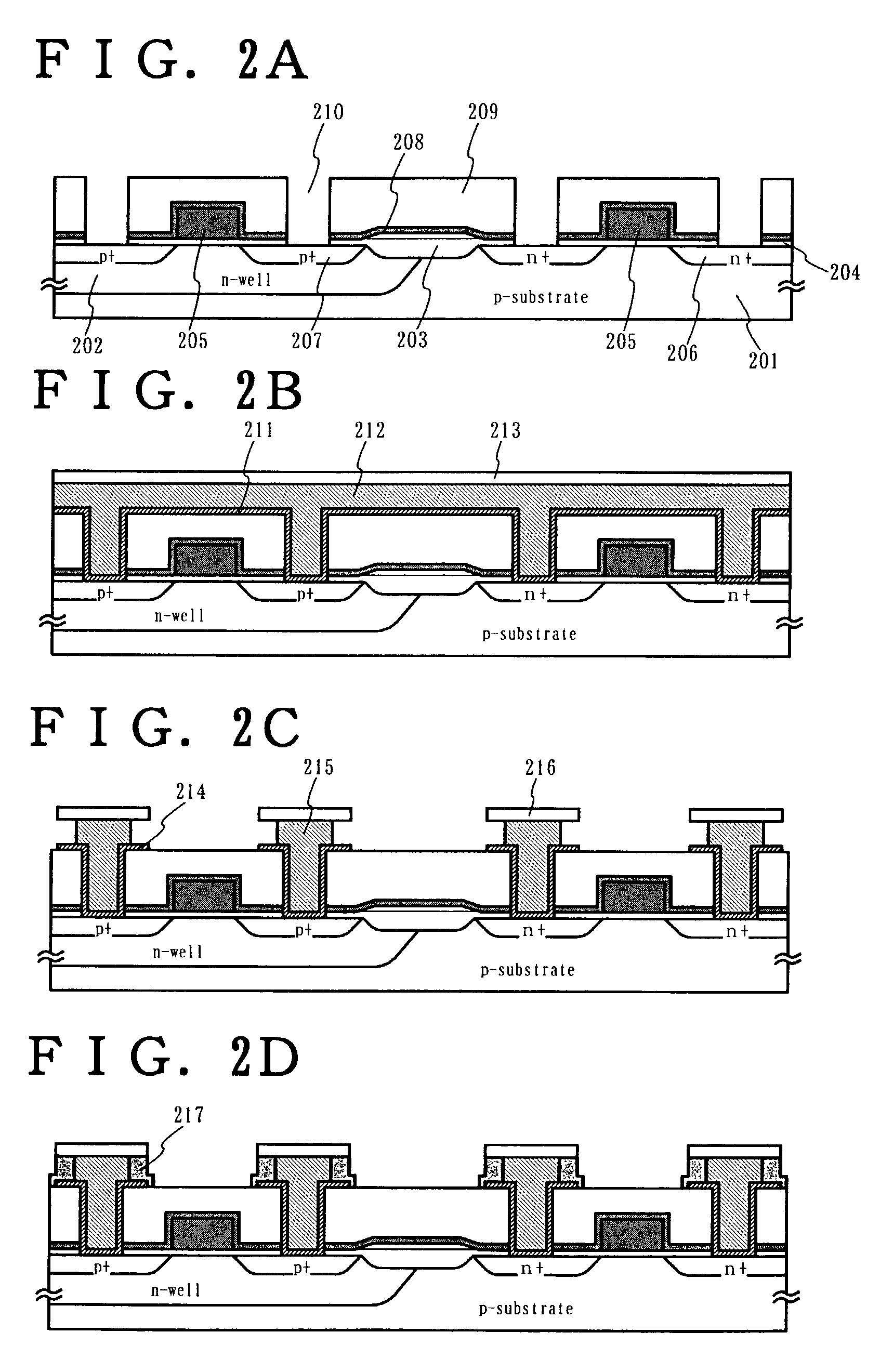
[0113] Embodiment 1
[0114] This embodiment gives with reference to FIGS. 4A to 10B a specific description on a method of manufacturing an active matrix liquid crystal display device employing a gate electrode and a wire of the present invention. In this embodiment, a crystalline silicon film crystallized by utilizing a catalytic element is used for a semiconductor layer that serves as an active layer of a TFT instead of a usual polycrystalline silicon film.
[0115] First, a first layer silicon oxynitride film 402a with a thickness of 50 nm and a second layer silicon oxynitride film 402b with a thickness of 100 nm are formed by plasma CVD on a glass substrate 401. The films 402a and 402 have different composition ratios and together make a base film 402. The glass substrate 401 used here is formed of quartz glass, barium borosilicate glass, or alumino borosilicate glass. On the base film 402 (402a and 402b), an amorphous silicon film 403a is formed by plasma CVD to a thickness of 53 nm....
embodiment 2
[0138] Embodiment 2
[0139] The present invention will be described specific examples of electronic apparatuses incorporated with the semiconductor device witch applied low resistance for wirings of the present invention. Note that, the term semiconductor device refers to a device in general that utilizes semiconductor characteristics to function, and includes the semiconductor display devices in which a LSI manufactured on a semiconductor substrate and a TFT manufactured on a transparent insulating substrate are used to construct a circuit, etc. The LSI is mainly classified into a memory LSI such as a DRAM and a logic LSI such as a CPU, and such LSIs are applied to constituent parts of various electronic apparatuses. The semiconductor display device includes an active matrix type liquid crystal display device, an EL display device and the like and is applied to a display portion of electric apparatuses in various kinds. Specific examples of electronic apparatuses in which the semicon...
PUM
| Property | Measurement | Unit |
|---|---|---|
| wavelength | aaaaa | aaaaa |
| temperature | aaaaa | aaaaa |
| temperature | aaaaa | aaaaa |
Abstract
Description
Claims
Application Information