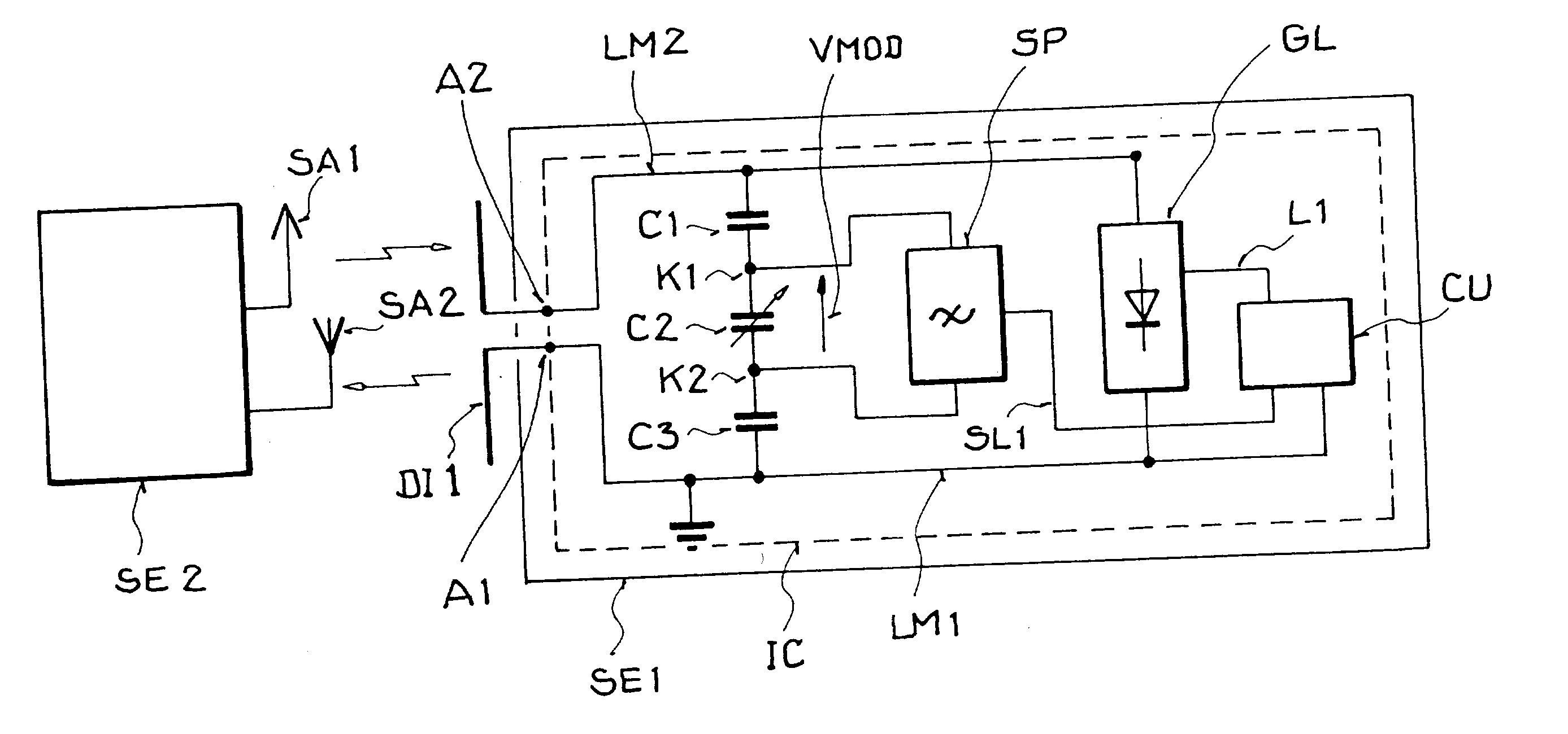
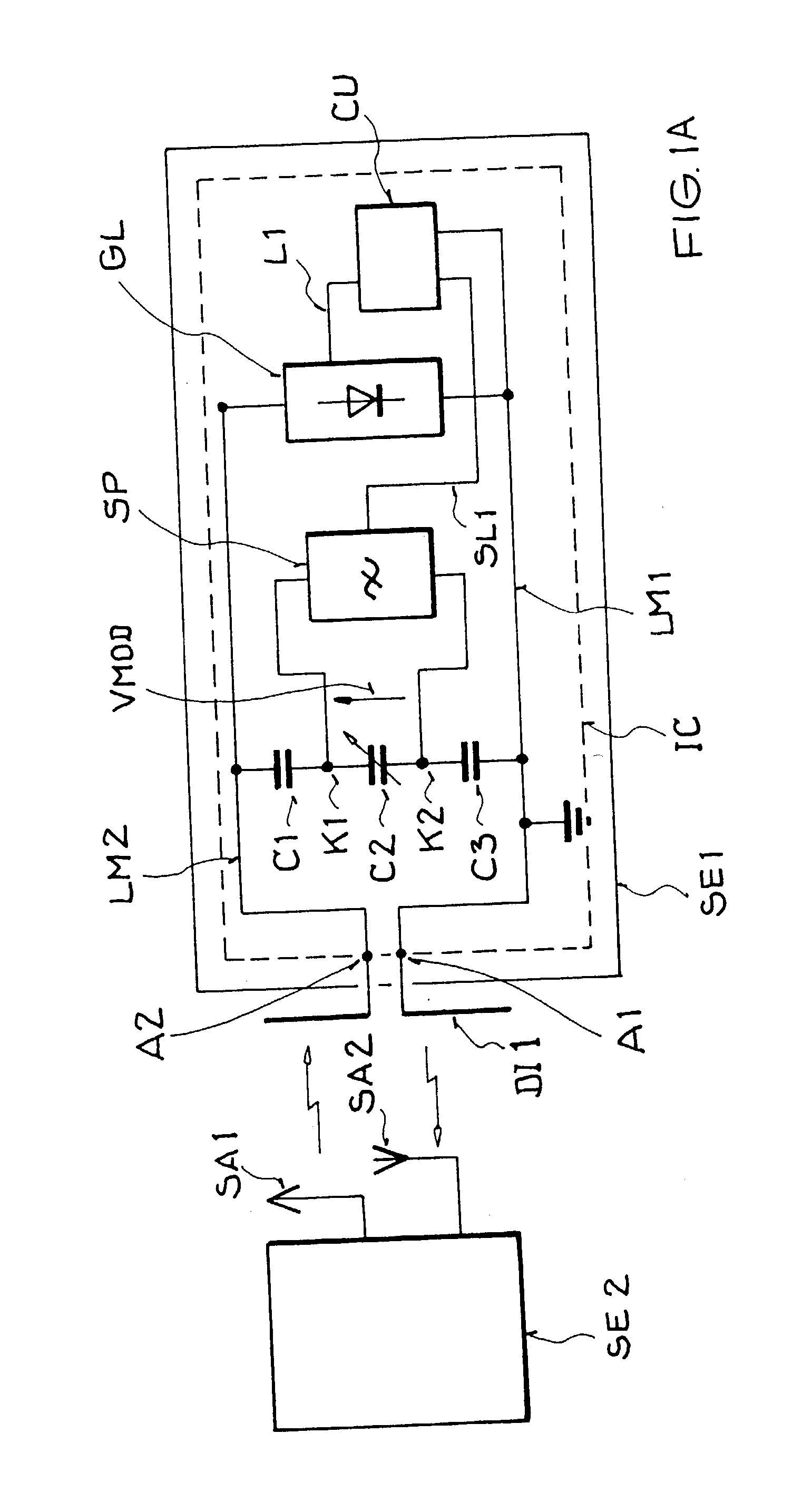
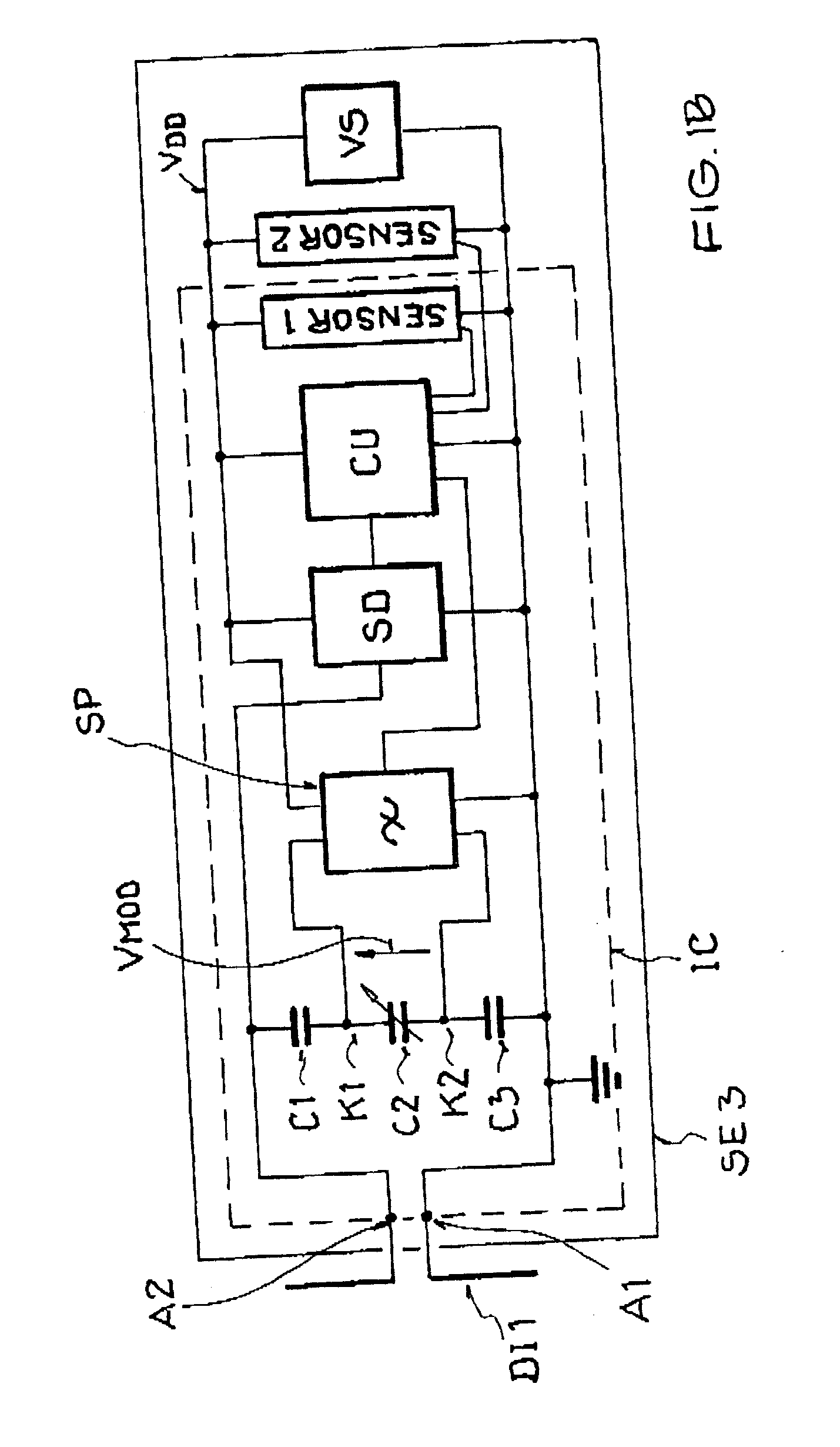
[0006] According to the invention, the impedance (and particularly mainly the imaginary part of the impedance) of the input antenna circuit can be easily varied with low losses in the receiving / backscattering arrangement. Thereby, the receiving / backscattering arrangement receives an interrogation signal, and modulates at least a portion of the received interrogation signal by changing the phase, to form a modulated answer or response signal having a changed phase, which is backscattered from the receiving / backscattering arrangement. The series arrangement of the first, second and third capacitances connected between the two antenna contacts controls the modulation of the backscattered portion of the interrogation signal. Particularly, this controlled modulation is achieved by the varactor that embodies the second
capacitance, which is arranged in series between the first and third capacitances. The varactor is controlled to vary its impedance (and particularly the imaginary part thereof), so that it phase-shift modulates and backscatters a portion of the received
signal on the conductor lines connected to the antenna contacts. The series connection of the three capacitances, with the variable capacitance varactor in the middle, ensures that the varactor is DC-decoupled from the antenna contacts between the first and third capacitances, which are embodied, for example, as normal capacitors each respectively having a fixed capacitance.
[0008] One
advantage of the inventive receiving / backscattering arrangement is that the impedance and thus the backscattering power can be varied especially effectively for a
data transmission in the
high frequency range, for example at 868 MHz, in that the parasitic losses are minimized. Investigations and experiments conducted by the applicants have shown that the quality or
Q factor of the antenna resonant circuit can be considerably increased by providing the MOS varactor as the second capacitance in the above mentioned series connection of three capacitances. Thereby, the communication range is increased. Furthermore, the first and third capacitances suppress an influence on the antenna circuit when applying a modulation voltage to the varactor, because the frequency of the modulation voltage is substantially smaller than the frequency of the
carrier signal. An additional
advantage is that the integration of the capacitances into the
integrated circuit with the other components of the antenna circuit considerably reduces the costs for the overall fabrication of the receiving / backscattering arrangement.
[0009] In a further detailed development of the receiving / backscattering arrangement, the integrated circuit arrangement particularly includes a modulation controller or controllable
voltage source for achieving the
impedance variation of the MOS varactor. In this manner, the backscattering power may especially advantageously be varied, whereby the backscattered portion of the interrogation signal, i.e. the response signal, comprises a phase modulated component. This is advantageous because a data transmission by means of a
phase modulation is less sensitive to interference or the like, than a data transmission by means of load or
amplitude modulation. Investigations conducted by the applicant have shown that a reliable data transmission and a high data
transmission rate can especially be achieved when the imaginary
phase modulation components are symmetrical with respect to the real part axis.
[0010] According to a further embodiment feature of the inventive receiving / backscattering arrangement, it is advantageous to construct the first and third capacitances from three respective stacked conductive
layers applied on a
semiconductor substrate. More particularly, a
dielectric layer is arranged between the first and second conductive
layers, and an insulating layer is arranged between the second and third conductive
layers, while the third conductive layer is arranged on the
semiconductor substrate. The third conductive layer is advantageously connected in a
low impedance manner to a reference potential or voltage, e.g. ground. It is further advantageous that the third conductive layer has a larger surfacial extent or area size in comparison to the first or second conductive layers. The third conductive layer advantageously is a common layer for both the first and third capacitances. In this manner, the quality or
Q factor of the serial capacitance arrangement is increased and the communication range is extended.
[0012] The inventive receiving / backscattering arrangement is especially advantageously used as a passive transponder or
wireless sensor, that is to say a transponder or
wireless sensor which does not include a self-contained power source and does not include a physical connection to an external power source, but rather in which the energy required to supply its integrated circuit is extracted or absorbed from the
electromagnetic field of the interrogation signal emitted by the
base station, for example by a
rectifier connected to the antenna contacts to absorb and rectify a portion of the received interrogation signal. In such a passive transponder, even with all of the operating power being absorbed from the received
signal field, the series arrangement of the three capacitances according to the invention, in connection with the high circuit qualities or Q-factors, makes it possible to increase the communication range to several meters.
[0014] Furthermore, since the series circuit of the three capacitances that achieves the backscattering modulation is predominantly capacitive, the modulation is predominantly a phase shift modulation rather than an
amplitude modulation. This also contributes to an increased communication range, due to the improved signal to
noise ratios of a PSK (
phase shift keying) modulation in comparison to an ASK (
amplitude shift keying) modulation.


