
Multilayer structures as stable hole-injecting electrodes for use in high efficiency organic electronic devices

a polyaniline anode, stable technology, applied in the direction of solid-state devices, electric lighting sources, electric light sources, etc., can solve the problems of long operating life, high operating voltage, and insufficient lifetime of high-resistance polyaniline devices for many commercial applications,

Inactive Publication Date: 2003-08-07
PARKER IAN D +1
View PDF8 Cites 40 Cited by
  • Summary
  • Abstract
  • Description
  • Claims
  • Application Information

AI Technical Summary

Benefits of technology

[0016] The multilayer structure provides sufficiently high resistivity to avoid cross-talk in passively-addressed pixellated polymer emissive displays; the multilayer anode structure of this invention simultaneously provides the low operating voltages and the long operating lifetime required for pixellated polymer emissive displays in commercial applications.
[0017] This invention additionally provides an improved configuration for electronic devices such as pixellated polymer emissive displays. This configuration leads to high efficiency, long operating life PED's while at the same time avoids excessive cross talk. This invention relates generally to the use of the multilayer anode structure in such devices. Thus, in one aspect this invention provides an improved polymer emissive diode. This improved diode is made up of an active emissive polymer layer having a first side in contact with a cathode and a second side in contact with a transparent anode. The improvement involves a multilayer transparent anode itself made up of a high conductivity transparent first contact layer, a transparent second layer in contact with the first contact layer and a third layer in contact with the second layer and the active emissive polymer layer. The second layer contains conjugated conductive organic polymer blend and has a high resistance. The third layer is thin and contains a conductive organic polymer having a lower resistance than the material of the second layer.

Problems solved by technology

Structures which favor high conductivity and thus high efficiency and long operating life are contrary to the conditions preferred for low cross talk.
However, the lifetime of such high resistivity polyaniline devices is not sufficient for many commercial applications.
Moreover, devices fabricated with polyaniline-layer-containing anodes require high operating voltages.
The resulting interpixel current leakage significantly reduces the power efficiency and limits both the resolution and the clarity of the display.
Making the polyaniline sheet resistance higher by reducing the film thickness is not a good option since thinner films give lower manufacturing yield caused by the formation of electrical shorts.
However, for use in pixellated displays, the PEDT layer needs to have a high electrical sheet resistance, otherwise lateral conduction causes cross-talk between neighboring pixels, and the resulting inter-pixel current leakage significantly reduces the power efficiency and limits both the resolution and the clarity of the display.

Method used


Image

  • Multilayer structures as stable hole-injecting electrodes for use in high efficiency organic electronic devices
  • Multilayer structures as stable hole-injecting electrodes for use in high efficiency organic electronic devices
  • Multilayer structures as stable hole-injecting electrodes for use in high efficiency organic electronic devices

Examples


example 1

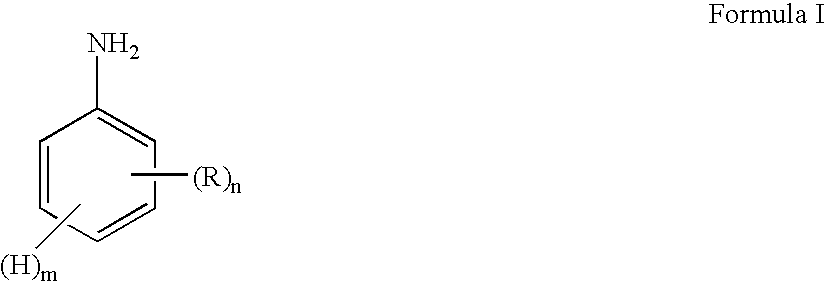
[0171] PANI(ES) was prepared according to the following reference (Y. Cao, et al, Polymer, 30 (1989) 2307). The emeraldine salt (ES) form was verified by the typical green color. HCl in this reference was replaced by poly(2-acrylamido-2-methyl-1-propanesulfonic acid (PAAMPSA) (Aldrich). First, 30.5 g (0.022 mole) of 15% PAAMPSA in water (Aldrich ) was diluted to 2.3% by adding 170 ml water. While stirring, 2.2 g (0.022M) aniline was added into the PAAMPSA solution. Then, 2.01 g (0.0088M) of ammonium persulfate in 10 ml water was added slowly into the aniline / PAAMPSA solution under vigorous stirring. The reaction mixture was stirred for 24 hours at room temperature. To precipitate the product, PANI(ES), 1000 ml of acetone was added into reaction mixture. Most of acetone / water was decanted and then the PANI(ES) precipitate was filtered. The resulting gum-like product was washed several times with acetone and dried at 40.degree. C. under dynamic vacuum for 24 hours.

[0172] This Example ...

example 2

[0173] Four grams (4.0 g) of the PANI(ES) powder prepared in Example 1 was mixed with 400 g of deionized water in a plastic bottle. The mixture was rotated at room temperature for 48 hours. The solutions / dispersions were then filtered through 1 .mu.m polypropylene filters. Different concentrations of PANI(ES) in water are routinely prepared by changing the quantity of PANI(ES) mixed into the water.

[0174] This Example demonstrates that PANI(ES) can be dissolved / dispersed in water and subsequently filtered through a 1 .mu.m filter.

example 3

[0175] A poly(ethylenedioxythiophene), PEDT (Baytron P. special grade, commercially available from Bayer), solution was diluted with an equal amount deionized water. The solution was stirred at room temperature overnight. The PEDT content of the solution was 0.8%. PEDT solutions were also prepared in which the content of PEDT was 0.4, 0.2 and 0.16%, respectively. All these solutions can be filtered through a 0.231 .mu.m filter.


PUM

PropertyMeasurementUnit
conductivityaaaaaaaaaa
thicknessaaaaaaaaaa
thicknessaaaaaaaaaa

Abstract

Multilayer anode structures (104) for electronic devices (100) such as polymer light-emitting diodes are described. The multilayer anodes include a high conductivity organic layer (114) adjacent to the photoactive layer (102) and a low conductivity organic layer (112) between the high conductivity organic layer and the anode's electrical connection layer (110). This anode structure provides polymer light emitting diodes which exhibit high brightness, high efficiency and long operating lifetime. The multilayer anode structure of this invention provides sufficiently high resistivity to avoid cross-talk in passively addressed pixellated polymer emissive displays; the multilayer anode structure of this invention simultaneously provides long lifetime for pixellated polymer emissive displays.

Description

[0001] This invention relates to organic electronic devices. More particularly it concerns multilayer hole-injecting electrodes (anodes) for electronic devices.DESCRIPTION OF PRIOR ART[0002] Organic electronic devices, such as light emitting devices, photodetecting devices and photovoltaic cells, may be formed of a thin layer of electroactive organic material sandwiched between two electrical contact layers. Electroactive organic materials are organic materials exhibiting electroluminescence, photosensitivity, charge (hole or electron) transport and / or injection, electrical conductivity, and / or exciton blocking. The material may be semiconductive. At least one of the electrical contact layers is transparent to light so that light can pass through the electrical contact layer to or from the electroactive organic material layer. Other devices with similar structures include photoconductive cells, photoresistive cells, photodiodes, photoswitches, transistors, capacitors, resistors, che...

Claims


Application Information

Patent Timeline
Patent Type & Authority Applications(United States)
IPC IPC(8): H05B33/26H01L27/32H01L51/50H01L51/52
CPCH01L27/3281H01L51/5206H01L51/5088H10K59/17H10K50/171H10K59/80517H05B33/26H10K50/17H10K50/816
Inventor PARKER, IAN D.ZHANG, CHI
Owner PARKER IAN D
Learn More