Light emitting photonic crystals

a light-emitting, crystal-type technology, applied in the field of photonic crystals, can solve the problems of reduced photoluminescence intensity, non-uniform pore size distribution, limited active surface area, etc., and achieve the effects of enhancing the emitted light or even lasing, enhancing the emitted light, and increasing the intensity of the emitted ligh

Inactive Publication Date: 2003-08-07
HONEYWELL INT INC
View PDF1 Cites 59 Cited by
  • Summary
  • Abstract
  • Description
  • Claims
  • Application Information

AI Technical Summary

Benefits of technology

0050] The porous double metallic mesh has a number of applications such as for forming a high luminosity LED. By applying a voltage to the structure, ejection of holes and electrons from the two electrodes is induced that will recombine inside the middle semiconductor layer to provide light emitted from the sides. Compared to the current in-plane architecture of the LEDs, the proposed design has a great advantage due to its enormous surface area. Moreover, the structure is a photonic crystal at the same time. By tuning the position of the photonic band gap the frequency of the light emission (electroluminescence) can overlap with the band gap edge. As a result of the photon confinement effects and the very small group velocity at the band edge, a strong nonlinear enhancement of the emitted light or even lasing will occur. The intensity of the emitted light could be additionally increased by deposition of a dielectric mirror on one side of the sample. The photonic crystals can also be made tunable by changing the periodicity of the crystalline structure. This can be achieved by compressing or expanding the crystalline structure, which in turn changes its volume. This change in unit cell parameter can be accomplished by any of the various well-known methods that result in a change of materials dimension. Other examples are the application of an electric field for an electrostrictive or piezoelectric material; a temperature or pressure change for either a shape memory material; the electrically-induced change in dimensions; or a thermally-induced change. Depending on the choice of materials and operating conditions, these changes can be either reversibl...

Problems solved by technology

The current porous silicon LEDs use only a small fraction of the material due to power dissipation losses, limited active surface area, and non-uniform pore size distribution.
The existing porous silica devices however suffer from the problems of non-uniform pore size dis...

Method used


Image

  • Light emitting photonic crystals
  • Light emitting photonic crystals
  • Light emitting photonic crystals

Examples


example 2

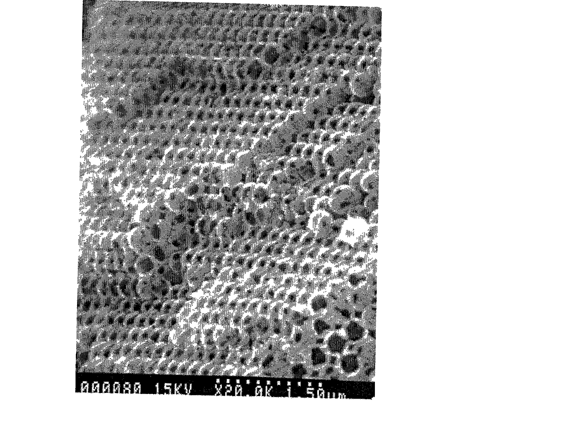
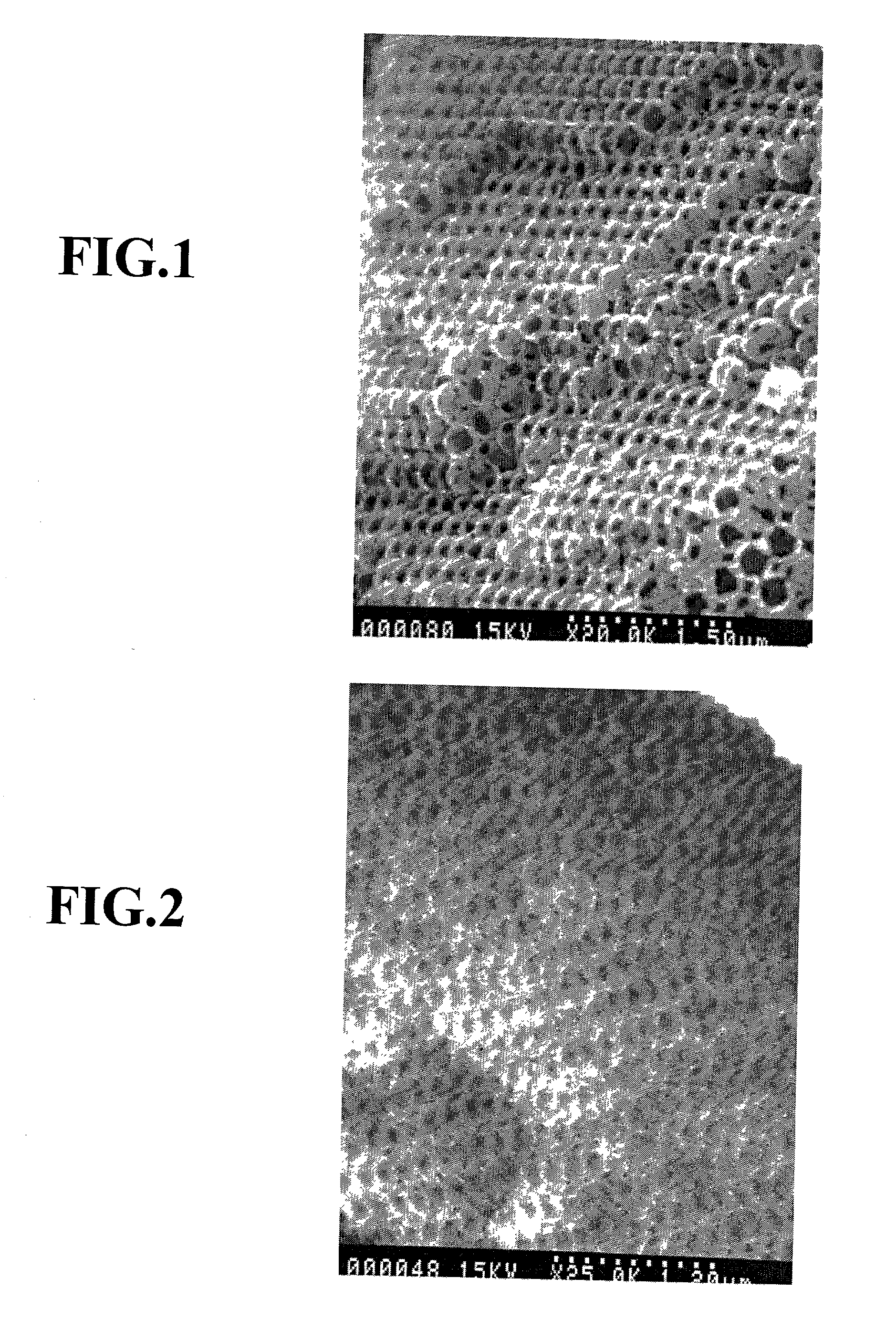
[0054] Production of Micropores. A monolayer of spheres is formed by loading a concave glass cell with a dilute silica suspension (.about.1 wt. % solids). After drying, this procedure is repeated several times with the same amount of dilute silica suspension to obtain an ordered film at the center of the cell comprising about 20 layers of silicon spheres. The spheres are sintered by heating a 650.degree. C. for five hours causing an attaching of adjacent spheres to one another by an intermediate neck thus forming a sintered porous opal. A sample of this opal is placed into the CVD chamber and evacuated to 10.sup.-3 mtorr. A precursor gas composed of 97% nitrogen and 3% silane (SiH.sub.4) is introduced into the CVD chamber. This precursor gas is delivered at a rate of 100 sccm per minute in order to maintain the pressure 400 mtorr. The temperature is maintained at 500.degree. C. and held at this temperature for 36 hours. Examination of the surface of this opal sheet shows that the si...

example 4

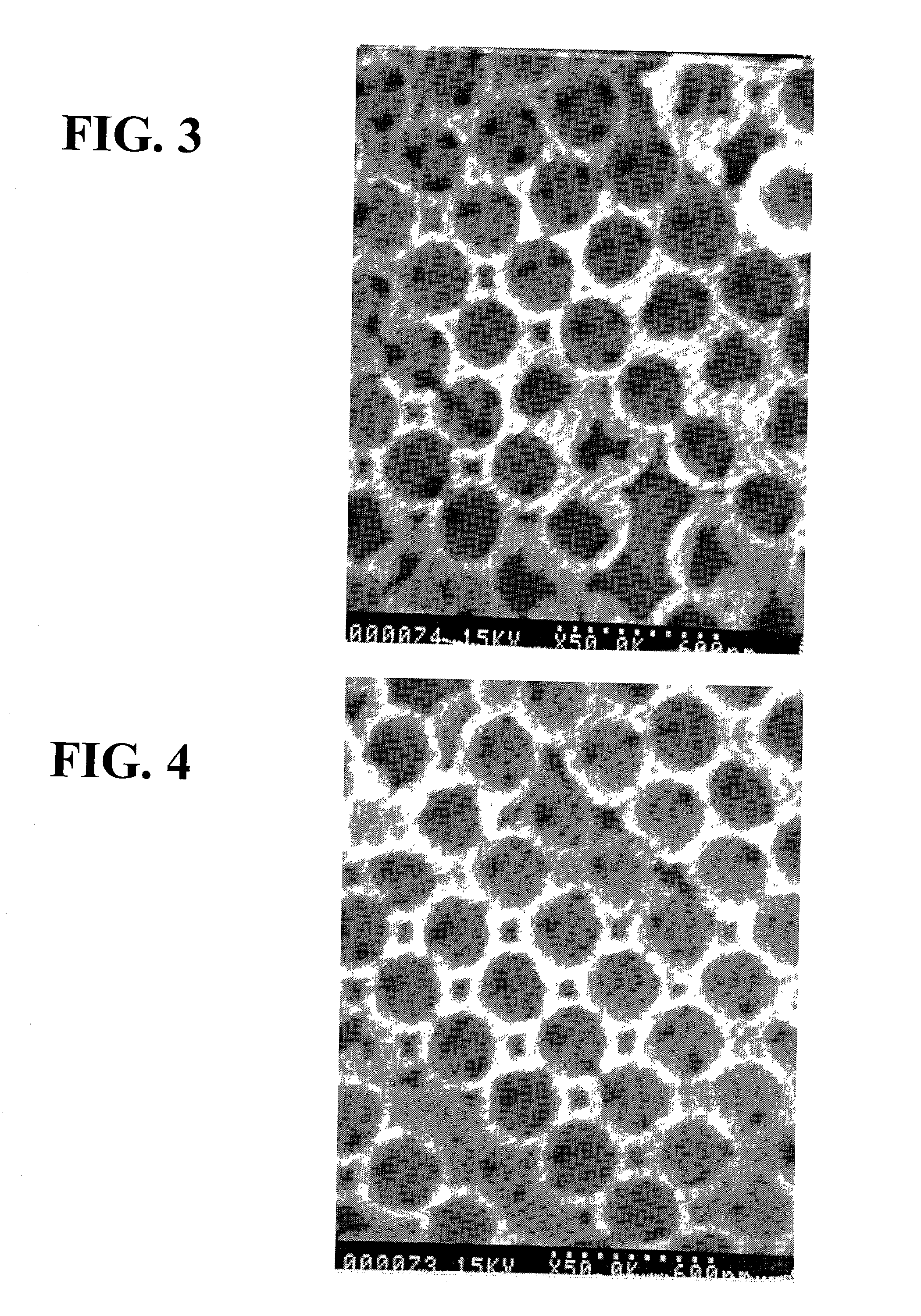
[0055] A photonic crystal having randomly nanoporous surface porosity is prepared by etching the microporous structure obtained from Example 1 with a 1:5:10 (by volume) or 4:1:5 (by volume) mixture of: HF (49%): HNO.sub.3 (70%): H.sub.2O (deionized). The first step in the process of creating nanoporosity involves the cleaning of the microporous sample by ultrasonication in pure ethanol. The chemical etching itself is done at room temperature (25.degree. C.) for 5-15 minutes. After the completion of the chemical etching, the sample is rinsed in deionized water for about 5 minutes and dried using pure nitrogen. The samples are then inspected under the photoluminescence test equipment. The photoluminescence testing involves illuminating the photonic crystal sample (that now has micro and random porosity) with light of 365 nm wavelength, using an UV lamp. During the illumination process the samples are viewed under a microscope. A bright red color (corresponding to photoluminescence) is...

example 5

[0056] A photonic crystal having randomly nanoporous surface porosity is prepared by etching the microporous structure obtained from Example 2 with HF vapor until randomly nanoporous surface porosity is obtained, which nanopores having an average pore diameter less than about 10 nm.


PUM

PropertyMeasurementUnit
Pore sizeaaaaaaaaaa
Thicknessaaaaaaaaaa
Thicknessaaaaaaaaaa

Abstract

The invention relates to processes for the synthesis of 2-D and 3-D periodic porous silicon structures and composites with improved properties having the advantages of porous silicon and photonic bandgap materials. Photonic crystals comprise a two dimensionally periodic or three dimensionally periodic microporous structural matrix of interconnecting, crystallographically oriented, monodispersed members having voids between adjacent members, and said members additionally having randomly nanoporous surface porosity. The silicon nanofoam material shows enhanced and spectrally controlled/tunable photoluminescence and electroluminesce and finds use as transparent electrodes, high-lumonosity light emitting diodes (LEDs), wavelength division multiplexors, high-active-area catalyst supports, photonic bandgap lasers, silicon-based UV detectors, displays, gas sensors, and the like.

Description

[0001] 1. Field of the Invention[0002] The invention relates to 2 and 3-dimensionally periodic porous structures and composites with improved properties incorporating the advantages of porous silicon and photonic bandgap materials. The inventive material, referred to as silicon nanofoam, shows enhanced and spectrally controlled, tunable photoluminescence and electroluminesce and finds use as high-luminosity light emitting diodes (LEDs), wavelength division multiplexors, high-active-area catalyst supports, photonic bandgap lasers, silicon-based UV detectors, displays, gas sensors, and the like.[0003] 2. Description of Related Art[0004] Photonic bandgap materials, also referred to as photonic crystals, and the possibility to utilize them to manipulate light was introduced first by Yablonovitch, Phys. Rev. Lett. 58, 2059-2062 (1987) "Inhibited spontaneous emission in solid-state physics and electronics" and John; Phys. Rev. Lett. 58, 2486-2489 (1987); "Strong localization of photons in...

Claims


Application Information

Patent Timeline
IPC IPC(8): C30B5/00G02B6/122
CPCB82Y20/00G02B6/1225C30B29/60C30B5/00Y10T428/249981Y10T428/249974Y10T428/8305Y10T428/249979Y10T428/249953Y10T428/24999
Inventor PADMANABHAN, ARAVINDBAUGHMAN, RAY H.ZAKHIDOV, ANVAR A.LAZAROV, GUENADIY
Owner HONEYWELL INT INC
Why Eureka
Try Eureka