Fabrication system and a fabrication method of light emitting device

a technology of light-emitting devices and fabrication systems, which is applied in the direction of vacuum evaporation coating, crystal growth process, coating, etc., can solve the problems of inability to perform photolithography processes after deposition, easy oxidation and deterioration of el materials, and high cos

Inactive Publication Date: 2003-08-28
SEMICON ENERGY LAB CO LTD
View PDF98 Cites 105 Cited by
  • Summary
  • Abstract
  • Description
  • Claims
  • Application Information

AI Technical Summary

Problems solved by technology

The EL materials tend to be deteriorated extremely, which are easily oxidized and deteriorated by the existence of oxygen or moisture.
On this account, photolithography processes cannot be performed after deposition.
Moreover, because of the wide space between the substrate and the evaporation source, the deposition rate becomes slow, the time required to exhaust the inside of the film-formation chamber takes long time, and throughput drops.
In addition, in the traditional evaporation apparatus, the utilization efficiency for expensive EL materials is about one percent or below, which is extremely low to cause the fabrication costs of the light emitting device to be extremely high.
The EL materials are very expensive, and the unit price per gram is far more expensive than the unit price per gram for gold.
However, in the traditional evaporation apparatus, the utilization efficiency for expensive EL materials is low.
Downsizing reduces the capacity of the film-formation chamber.
It is also considered that the degree of sealing the container for storing the EL material is not enough.
More specifically, oxygen, moisture and other impurities are likely to be mixed, which are one cause of deteriorating the EL element.
However, when the pretreatment chamber is equipped with the gloves, the chamber cannot be vacuumed, and thus the operation is done at an atmospheric pressure.
Even though the operation is done in a nitrogen atmosphere, it has been difficult to reduce moisture and oxygen in the pretreatment chamber as much as possible.
However, the evaporation material is powder, and thus it is difficult to manufacture a transfer robot.
Therefore, it has been difficult to manufacture a total closed system allowing that the process steps from the step of forming the EL layer over a lower electrode to the step of forming an upper electrode are all automated to avoid impurities from being mixed.
Moreover, even though the highly purified EL materials are provided by the material manufacturer, the traditional transfer operation in the light emitting device manufacturer always has the risk of mixing impurities not to keep the purity of EL materials, which has given a limit in the purity.

Method used


Image

  • Fabrication system and a fabrication method of light emitting device
  • Fabrication system and a fabrication method of light emitting device
  • Fabrication system and a fabrication method of light emitting device

Examples


embodiment

[0063] Embodiment

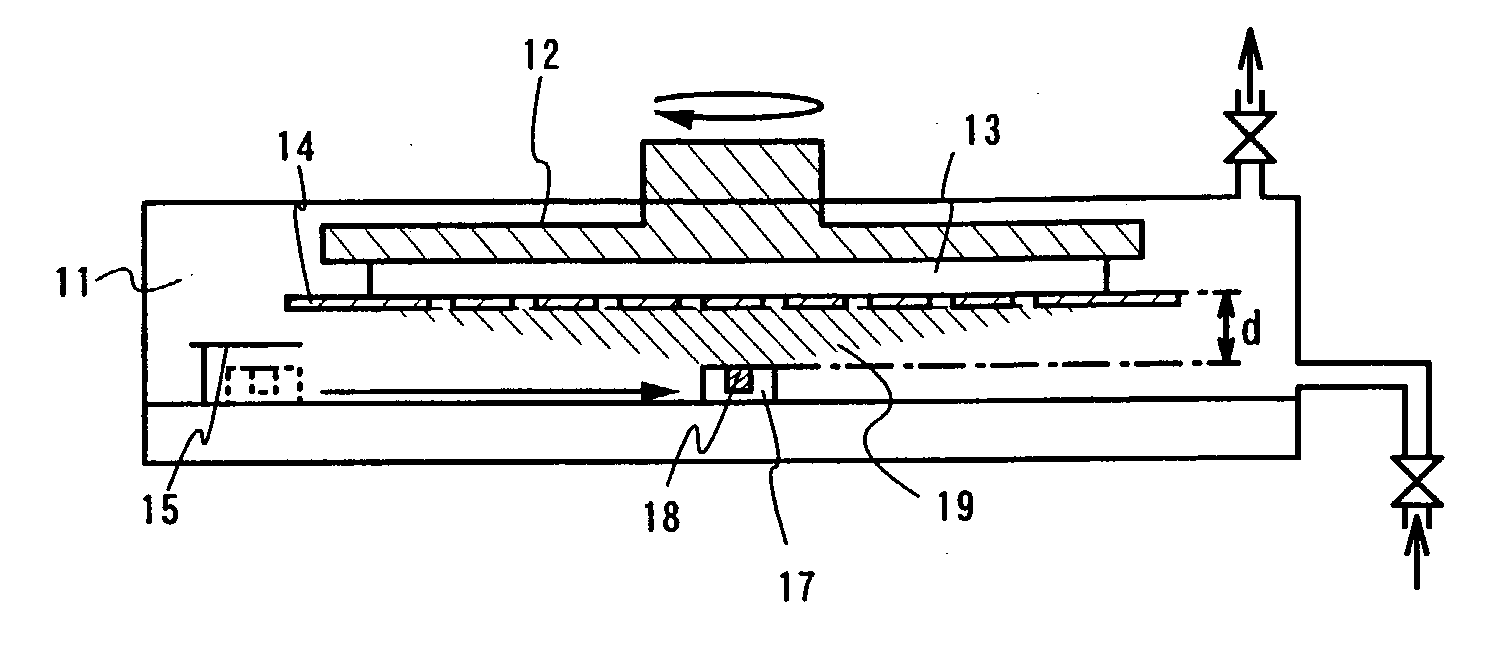
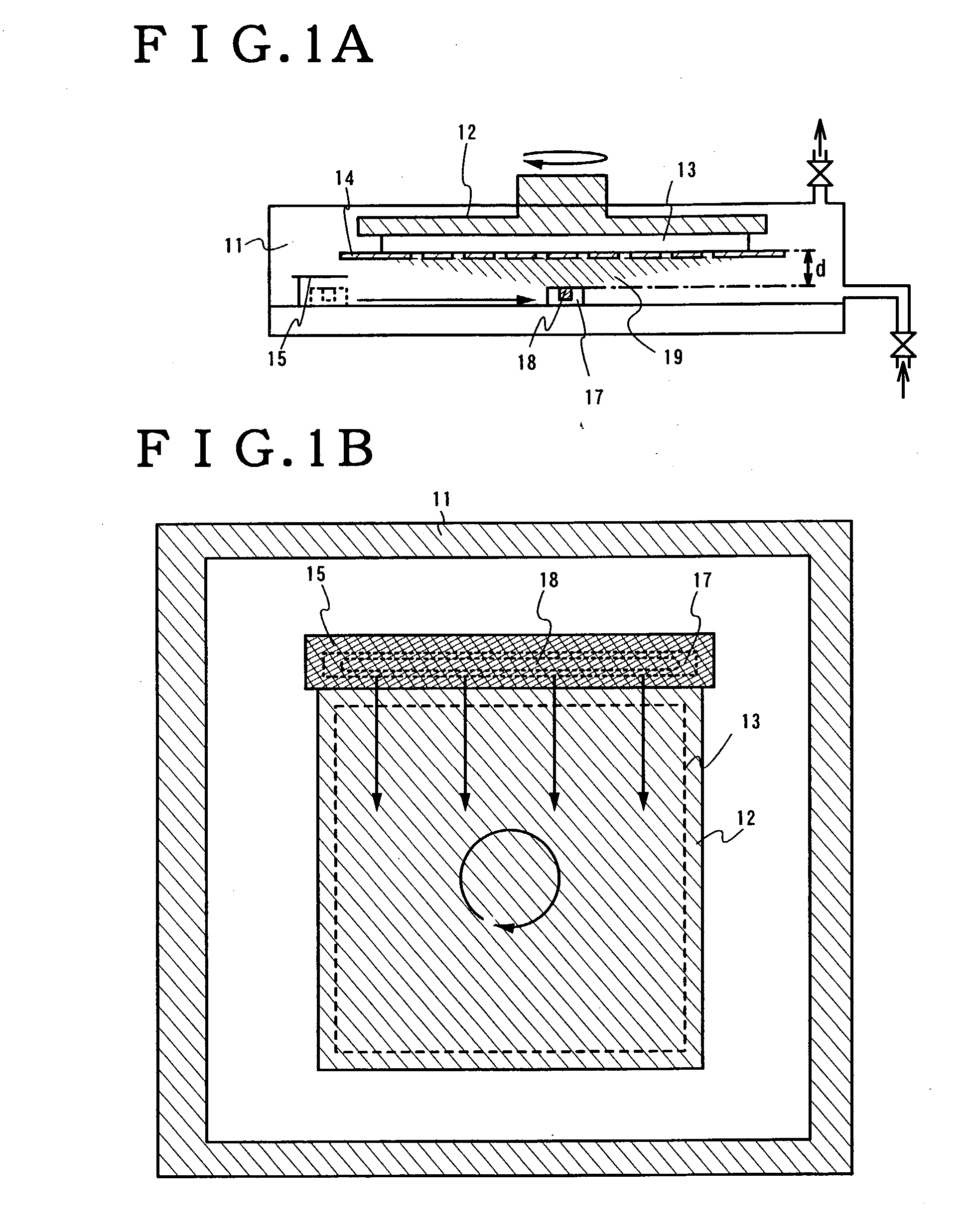
[0064] FIGS. 1A and 1B show a deposition apparatus of the invention. FIG. 1A is a cross section, and FIG. 1B is a top view.

[0065] In FIGS. 1A and 1B, reference numeral 11 denotes a film-formation chamber, reference numeral 12 denotes a substrate holder, reference numeral 13 denotes a substrate, reference numeral 14 denotes a mask, reference numeral 15 denotes a deposition shield (deposition shutter), reference numeral 17 denotes an evaporation source holder, reference numeral 18 denotes an evaporation material, and reference numeral 19 denotes an evaporated evaporation material.

[0066] Evaporation is conducted in the film-formation chamber 11 vacuumed at a vacuum degree of 5.times.10.sup.-3 Torrs (0.665 Pa) or below, preferably vacuumed to 10.sup.-4 to 10.sup.-6 Pa. In evaporation, the evaporation material is evaporated (vaporized) by resistance heating beforehand. A shutter (not shown) is opened when evaporation, which causes the material to fly in the direction of ...

example

Example 1

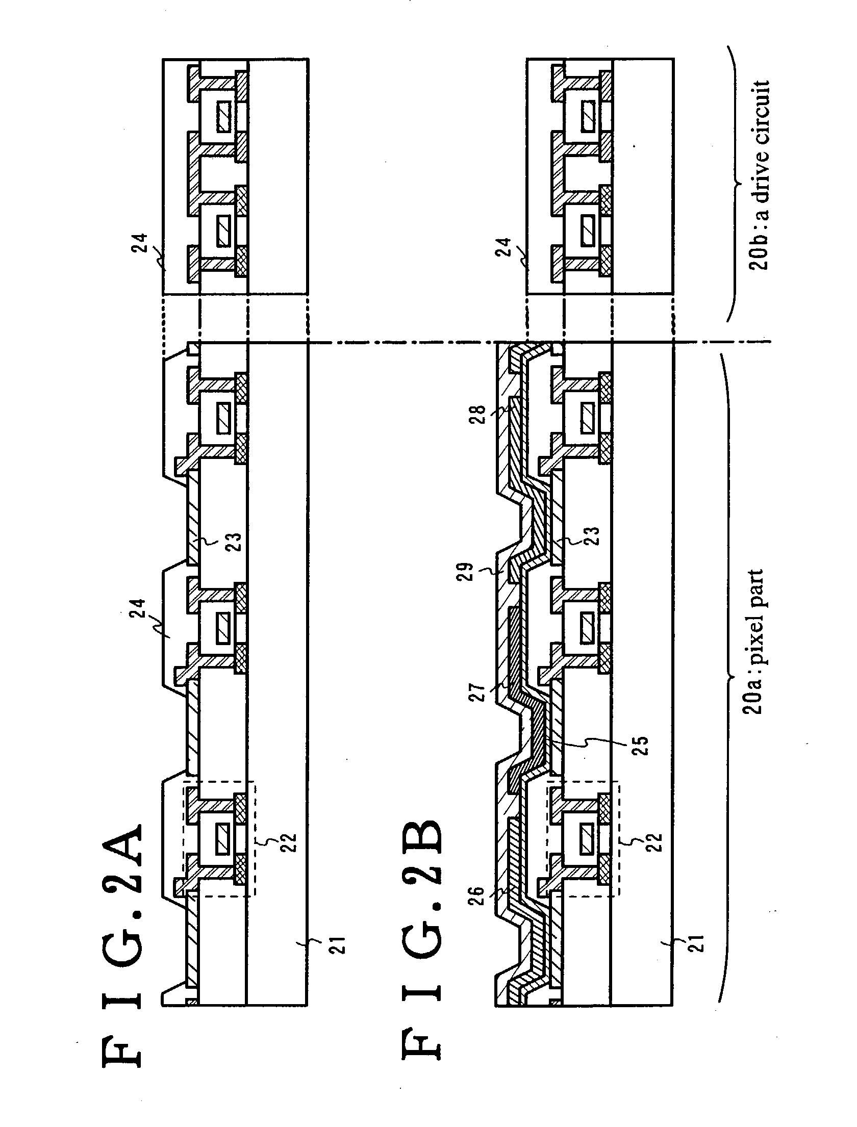
[0080] Here, the process steps of fabricating an active matrix light emitting device having a pixel part and a drive circuit on the same substrate and including an EL element is exemplified and described in FIGS. 2A and 2B.

[0081] First, as shown in FIG. 2A, a thin film transistor (hereafter, it is called a TFT) 22 is formed over a substrate 21 having an insulated surface by publicly known fabrication process steps. In a pixel part 20a, an n-channel TFT and a p-channel TFT are formed. Here, the p-channel TFT for feeding current to an organic light emitting element is illustrated in the drawing. It is acceptable that the TFT for feeding current to the organic light emitting element is the n-channel TFT or the p-channel TFT. In a drive circuit 20b disposed around the pixel part, the n-channel TFT, the p-channel TFT, and a CMOS circuit that complementally combines them are formed. Here, an example is shown in which an anode 23 formed of a transparent conductive oxide film (ITO ...

example 2

[0093] FIG. 3 is a diagram illustrating the appearance of the top view of an E1 module. In a substrate (it is also called a TFT substrate) 35 where a countless number of TFTs are formed, a pixel part 30 for display, drive circuits 31a and 31b for driving the pixels in the pixel part, connecting parts for connecting a cathode disposed over an EL layer to interconnect wiring lines, and terminal parts 32 for bonding an FPC to connect external circuits are disposed. The module is sealed with a substrate for encapsulating the EL element and a sealing material 34.

[0094] In FIG. 3, the cross section of the pixel part is not defined particularly. Here, the cross section shown in FIG. 2B is exemplified. The module shown in FIG. 3 is a product after the encapsulation process in which a protection film or an encapsulation substrate was bonded to the product having the cross sectional structure shown in FIG. 2B.

[0095] An insulating film is formed over the substrate, and the pixel part and the d...


PUM

PropertyMeasurementUnit
distanceaaaaaaaaaa
distanceaaaaaaaaaa
distanceaaaaaaaaaa

Abstract

An evaporation apparatus with high utilization efficiency for EL materials and excellent film uniformity is provided. The invention is an evaporation apparatus having a movable evaporation source and a substrate rotating unit, in which the space between an evaporation source holder and a workpiece (substrate) is narrowed to 30 cm or below, preferably 20 cm, more preferably 5 to 15 cm, to improve the utilization efficiency for EL materials. In evaporation, the evaporation source holder is moved in the X-direction or the Y-direction, and the workpiece (substrate) is rotated for deposition. Therefore, film uniformity is improved.

Description

[0001] 1. Field of the Invention[0002] The present invention relates to a fabrication apparatus having a deposition apparatus for use in deposition of materials allowed to be deposited by evaporation (hereafter, they are called evaporation materials). Particularly, the invention is an effective technique when organic materials are used as the evaporation materials.[0003] 2. Description of the Related Art[0004] In recent years, the research of light emitting devices having EL elements as self-luminous elements has been conducted actively. In particular, a light emitting device using organic materials as EL materials is receiving attention. The light emitting device is also called an organic EL display or an organic light emitting diode.[0005] In addition, the EL element has an anode, a cathode, and a layer containing organic compounds where an electric field is applied to obtain electroluminescence (hereafter, it is denoted by EL layer). Electroluminescence in the organic compounds h...

Claims


Application Information

Patent Timeline
Patent Type & Authority Applications(United States)
IPC IPC(8): C23C14/12C23C14/24C23C14/50
CPCC23C14/12C23C14/505C23C14/24H05B33/10
Inventor YAMAZAKI, SHUNPEIMURAKAMI, MASAKAZUOHTANI, HISASHI
Owner SEMICON ENERGY LAB CO LTD
Why Eureka
Try Eureka